PCB Rules and Violations
Contents
Parent page: PCB Panels

Browse, edit and interactively view design rules and their associated violations.
Summary
Design Rule Checking (DRC) is a powerful automated feature that checks both the logical and physical integrity of your design. The PCB Rules And Violations panel allows easy browsing of the enabled design rules and violations in the current board layout workspace. The panel provides a central point for browsing and editing rules, instigating design rules checks and viewing individual violations as graphic overlays in the editor workspace.
Panel Access
Access the PCB Rules And Violations panel by clicking Home | Design Rules| ![]() from the main menu. The Rules And Violations panel becomes accessible when the the PCB Editor is active.
from the main menu. The Rules And Violations panel becomes accessible when the the PCB Editor is active.
Selecting Rules and Violations
The body of the PCB Rules And Violations panel has three sections, each offering a finer scope of the design rules and violations:
- Rule Classes – Design rules grouped by classes, such as Clearances and Widths.
- Rules – The individual design rules within the selected class. The specific Design Rule Check (DRC) can be run via the right-click menu.
- Violations – Details of each rule violation reported by activated design rules checks.
Selecting an individual rule violation causes the design workspace to graphically highlight that violation. Enhanced violation graphics are drawn only on the layers on which the offending primitives reside, and that layer (if enabled) will become the active layer in the workspace.
When the rule violations details are enabled (see below), the editor's graphics will display the constraint value defined for the rule and indicate how the offending primitive(s) are either below or above this value.
Violation of a minimum Width rule set to 11mil for Net LCD_DB7.
Violation of a Via dimension rule set to minimums of 50mil diameter and 28mil hole size.
Note that if you have the Zoom highlighting method enabled, the workspace will be zoomed-in to fit the browsed violation for a much more precise view of the violating area. The level of that zoom can be varied via the panel's Zoom Level button.
You can also directly view details of a violation from the PCB Rules and Violations panel or within the design workspace.
- In the panel, double click on a violation entry in the Violations list to open the Violation Details dialog.
- In the workspace, with the cursor over an offending primitive, right-click and select Violations from the context menu, then select the appropriate violation to open a Violation Details dialog.
The detailed information of the rule violations examples shown in workspace graphic images above.
See the Violation Details dialog page for more information.
Setting the visual filtering
The visual result of the panel selections on the document in the design editor window is determined by a series of highlighting controls toward the top of the panel. The effect that is imposed in the editor view can be set to Normal, Mask or Dim, where in practice, Mask has the most obvious highlighting effect.
The Normal / Mask / Dim dropdown list provides options for visibly contrasting filtered and unfiltered objects within the design editor window.
Select the type of visual filtering applied using the masking mode drop-down list.
The visual highlighting effect for each masking mode:
- Normal – Filtered objects are visible in the design editor window and the appearance of unfiltered objects remains unchanged.
- Mask – Filtered objects are highlighted in the design editor window, with all other objects made monochrome
- Dim – Filtered objects are highlighted in the design editor window, with all other objects retaining their colors, but shaded.
Click the ![]() button to confirm a visual filtering change and refresh the editor window.
button to confirm a visual filtering change and refresh the editor window.
Display control
In Mask view mode, unfiltered (not selected) objects are monochrome. To set the contrast of the background (un-highlighted) objects, use the Mask Level slider control available in the View | Highlight & Edit Mask group.
Similarly, in Dim view mode unfiltered objects retain their colors, but are shaded. Set the balance between filtered and unfiltered objects using the Dim Level slider available in the View | Highlight & Edit Mask group, as shown above.
Use the View | Highlight & Edit Mask | ![]() button or the panel's
button or the panel's ![]() button to remove the display highlighting.
button to remove the display highlighting.
Filter options
The panel's three checkboxes apply these filter actions:
- Select – when enabled, the filtered objects will be selected in the workspace.
- Zoom – when enabled (default), the filtered objects will be zoomed and centered (where possible) in the design editor window. Use the button to adjust the zoom factor that will be used to close-in on filtered objects.
- Clear Existing – when enabled (default), any existing filter will be cleared before applying a new one. Disabling this option allows you to extend an existing filter, essentially refining the filter further by applying a new filter in addition to the existing one.
Any combination of these options can be enabled. For example, you might want to have all filtered objects zoomed, centered and selected in the design editor window, whilst applying masking to take away the clutter of other design objects.
Use the ![]() button to disable the currently-applied filter. All objects in the design workspace will become fully visible and available for selection/editing. If you wish to re-apply the filter, click the
button to disable the currently-applied filter. All objects in the design workspace will become fully visible and available for selection/editing. If you wish to re-apply the filter, click the ![]() button.
button.
Controlling the Display of DRC Violations
The visual display of DRC violations can be configured to maximize clarity and/or suit your own preferences by setting the style, number and color of the graphic markers. Along with the graphic display of violation details, the design primitives can be overlaid with a graphic pattern selected from a number of styles.
Violation Display Preferences
Control over how DRC violations are displayed – using the custom violation graphics and/or a defined violation overlay – is specified on the PCB Editor – DRC Violations Display page of the Preferences dialog (File » ![]() button).
button).
Violation display Preferences settings are available to:
- Specify the overlay color style for highlighted Rule Violations – an overlaid pattern or color.
- Set how Violation display styles are handled when you zoom in and out – how a pattern or color displays with zoom levels, and with how much detail.
- Define a Violation display style for each type of Rule – enabling or disabling graphical violation details and overlay for each type.
See the DRC Violations Display Preferences page for more information.
Defining Violation Colors
To provide further flexibility when displaying rule violations in the workspace, the two violation display types – violation details and violation overlay – have separate associated system colors. This allows you to differentiate between the two using different, distinct colors.
Color assignment is performed in the View Configurations dialog – in 2D Layout Mode, click View | View | ![]() » View Configurations » View Configuration, or just press the L key.
» View Configurations » View Configuration, or just press the L key.
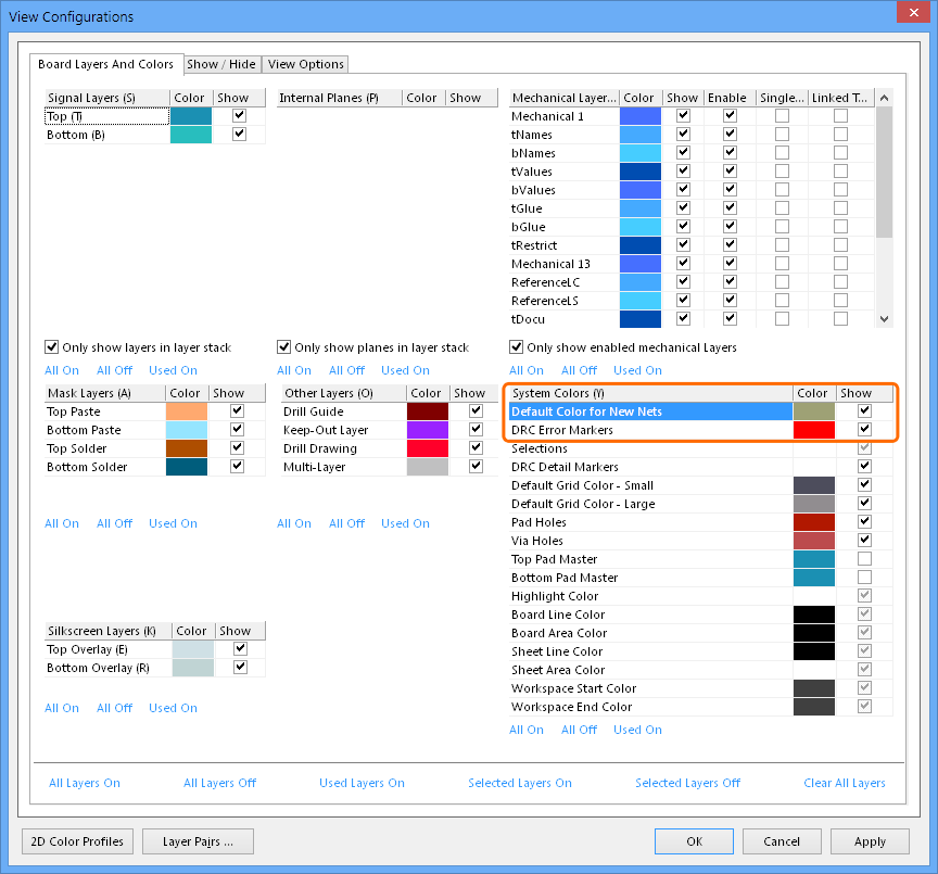
In the View Configurations dialog, specify different coloring for the two violation display types, and enable/disable their display, as required.
See the DRC Board Layers and Colors dialog page for more information.
Right-Click Menus
The entries in each section of the PCB Rules And Violations panel offer a range of options via the right-click context menu. Notable right-click options for each section are:
Rule Classes
- Run DRC Rule Class – Runs all rules contained in the class. Classes may contain a single rule (such as Short-Circuit Constraint) or a large number (typically, the Clearance Constraint class).
- Clear Violations For Rule Class – Clears the violations (both graphically and listed in the panel) for all rules contained in the class. Use the button to reset workspace highlighting.
Rules
- Run DRC Rule – Runs the selected rule.
- Clear Violations – Clears the violations reported by the selected rule.
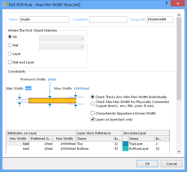
- Properties – Opens the Edit PCB Rule dialog, allowing the rule configuration to be changed on the fly. Equivalent of double-clicking on the rule name.
Rules can edited on the fly from the PCB Rules And Violations panel.
Violations
- Properties – Opens the Violation Details dialog, which provides full details of the rule constraint and the current violation. Equivalent of double-clicking on the violation entry.
- Zoom Selected – Zooms workspace to the selected violation(s). Useful when the Zoom checkbox option is not enabled.
Notes
- For full access to the PCB Constraint Classes and Rules, open the PCB Rules and Constraints Editor dialog from the Home | Design Rules | button.
- Online Design Rule Checking can be enabled/disabled in the PCB Editor - General page of the Preferences dialog; File »
- Design Rules can be individually enabled for Online or Batch checking (or both) in the Design Rule Checker dialog – Home | Design Rules | button.