Keepout
Contents
Parent page: PCB Objects

Two fills; the left one placed on the Keepout layer as an all-layer keepout, the right one placed on the Top
Layer as a layer-specific keepout.
Summary
A keepout is the name given to an object that blocks or prevents the placement of copper objects within an area. A keepout can be defined as a fence (in essence, a wall around the area to be protected) or they can be defined as a solid area of keepout that completely covers the area to be protected.
Availability
Define a keepout area by placing standard design objects, such as Fills, Tracks, and Regions to create the required shape.
Placement
There are two approaches to defining a Keepout:
- All-layer keepout — place an object, such as a fill, track or region, on the Keepout layer; these objects then create a keepout on all signal layers.
- Layer-specific keepout — place a layer-specific keepout object on a signal layer. It creates a keepout on only that signal layer. Keepout objects are simply standard design objects with the Keepout checkbox enabled in the object's properties dialog. Layer-specific keepout objects have the color of that layer, with a thick outline shown in the current keepout color. Layer-specific keepouts are not included in generated outputs, such as Gerber or ODB++.
For more information on layer-specific keepouts, refer to the relevant object.
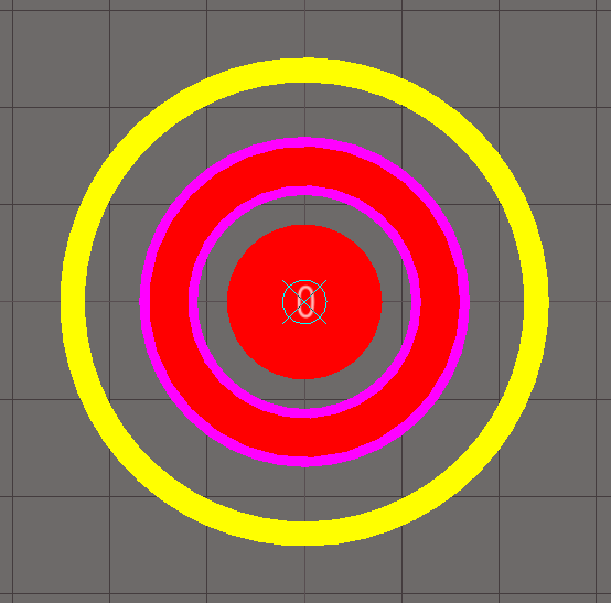
A typical design for a Fiducia): the inner red circle is a top layer pad, the surrounding
red & purple circle is a Keepout arc.