Fill
Contents
Parent page: PCB Objects

A placed Fill
Summary
A fill is a rectangular object that can be placed on any layer. When placed on a signal layer, a fill becomes an area of solid copper that can be used to provide shielding or to carry large currents. Fills of varying size can be combined to cover irregularly shaped areas, and can also be combined with track or arc segments and be connected to a net.
Fills can also be placed on non-electrical layers. For example, place a fill on the Keep-Out layer to designate a 'no-go' area for autorouting. Place a fill on a Power Plane, Solder Mask, or Paste Mask layer to create a void on that layer. In the PCB Library Editor, fills can be used to define component footprints.
Availability
Fills are available for placement in both PCB and PCB Library Editors:
- PCB Editor - click Home | Place | from the main menus.
- PCB Library Editor - click Home | Place | » Fill from the main menus.
Placement
After launching the command, the cursor will change to a cross-hair and you will enter fill placement mode. Placement is made by performing the following sequence of actions:
- Click or press Enter to anchor the first corner of the fill.
- Move the cursor to adjust the size of the fill, then click or press Enter to anchor the diagonally-opposite corner and complete placement of the fill.
- Continue placing further fills, or right-click or press Esc to exit placement mode.
Additional actions that can be performed during placement are:
- Press the L key to flip the fill to the other side of the board – note that this is only possible prior to anchoring the fill's first corner.
- Press the + and - keys (on the numeric keypad) to cycle forward and backward through all visible layers in the design, respectively, to change placement layer quickly.
- Press the Tab key to access an associated properties dialog, from where properties for the fill can be changed on-the-fly.
Placing a Fill as a Keepout
A Fill can be placed as a layer-specific keepout object or an all-layer keepout to act, for example, as a placement or routing barrier. Objects defined as keepouts are ignored during output generation, such as photo plotting and printing. A layer-specific keepout fill is a Fill object with its Keepout property enabled; an all-layer keepout is a Fill that has been placed on the Keepout layer.
- To place a layer-specific keepout, either place a standard Fill on the required signal layer then enable the Keepout property to make it a layer-specific keepout, or use the predefined Fill keepout placement command available as follows:
- PCB Editor - click Home | Place | » Fill.
- PCB Library Editor - click Home | Place | » Keepout » Fill.
- PCB Editor - click Home | Place |
- To place an all-layer keepout, make the Keepout layer the active layer then place a standard Fill from the main menus.
Graphical Editing
This method of editing allows you to select a placed fill object directly in the workspace and change its size, shape or location graphically.
When a fill object is selected, the following editing handles are available:
A selected Fill
- Click and drag A to resize the fill in the vertical and horizontal directions simultaneously.
- Click and drag B to resize the fill in the vertical and horizontal directions separately.
- Click and drag C to rotate the fill about its center point.
- Click anywhere on the fill – away from editing handles – and drag to reposition it. While dragging, the fill can be rotated or mirrored:
- Press the Spacebar to rotate the fill counterclockwise or Shift+Spacebar for clockwise rotation. Rotation is in accordance with the value for the Rotation Step defined on the PCB Editor – General page of the Preferences dialog.
- Press the X or Y keys to mirror the fill along the X-axis or Y-axis respectively.
Non-Graphical Editing
The following methods of non-graphical editing are available:
Editing via an Associated Properties Dialog
Dialog page: Fill
This method of editing uses the following dialog to modify the properties of a fill object.
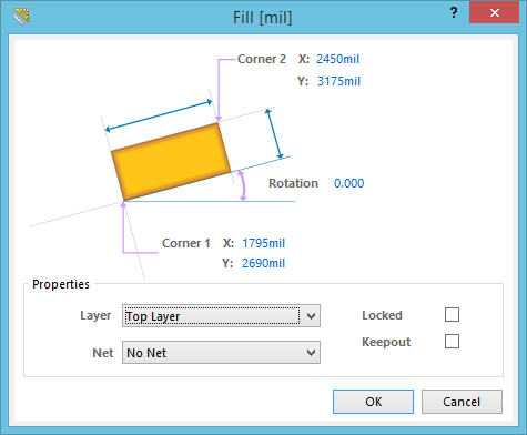
The Fill dialog
The Fill dialog can be accessed during placement by pressing the Tab key.
After placement, the dialog can be accessed in one of the following ways:
- Double-click on the placed fill object.
- Place the cursor over the fill object, right-click then choose Properties from the context menu.
Editing via an Inspector Panel
Panel pages: PCB Inspector, PCBLIB Inspector
An Inspector panel enables you to interrogate and edit the properties of one or more design objects in the active document. Used in conjunction with appropriate filtering, the panel can be used to make changes to multiple objects of the same kind, from one convenient location.