Component
Contents
Parent page: PCB Dialogs
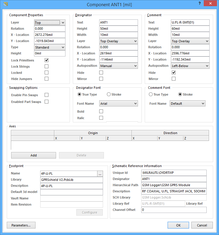
The Component dialog
Summary
The Component dialog is used to edit the properties of the selected component. The Component footprint defines the space and connection points needed to mount the physical component on the printed circuit board.
Access
The dialog can be accessed during Component placement after entering the required information in the Place Component dialog then by pressing the Tab key.
After placement, the dialog can be accessed in the following ways:
- Double-clicking on a Component.
- Placing the cursor over a Component, right-clicking then selecting the Properties command from the context menu.
Options/Controls
Component Properties
- Layer - Sets the layer on which the component is placed. Components can be assigned to the Top layer or Bottom layer. Click to select a different layer. Changing the layer status swaps all of the component primitives to each layer's respective opposite layer. For example, moving a Top layer component to the Bottom layer means: single layer pages are swapped from the Top to the Bottom layer; primitives on the Top Overlay are reassigned to the Bottom Overlay; and primitives on a paired mechanical layer are swapped to the other mechanical layer in that pair. The orientation of the component will be flipped along the X-axis and the component overlay text will read from the bottom. To flip a component during placement, press the L key while the component is floating on the cursor.
- Rotation - The component's angle of rotation (in degrees), measured counterclockwise from zero (the 3 o'clock horizontal). Edit to change the rotation of the component. Minimum angular resolution is 0.001°.
- X-Location - The current X (horizontal) coordinate of the reference point of the component relative to the current workspace origin. Edit to change the X position of the component. The value can be entered in either metric or imperial; include the units when entering a value whose units are not the current default. The current units used in the dialog can be toggled by pressing the Ctrl+Q shortcut. The reference point for a component footprint is set in the Library Editor.
- Y-Location - The current Y (vertical) coordinate of the reference point of the component relative to the current origin. Edit to change the Y position of the component. The value can be entered in either metric or imperial; include the units when entering a value whose units are not the current default. The current units used in the dialog can be toggled by pressing the Ctrl+Q shortcut. The reference point for a component footprint is set in the Library Editor.
- Type - Select one of the following component types for the component footprint here. The available types are:
- Standard - These components possess standard electrical properties, are always synchronized between the schematic and PCB (the footprint, pins/pads and net assignments must all match), and are included in the BOM. An example is a standard electrical component, such as a resistor.
- Mechanical - These components do not have electrical properties, are not synchronized (you must manually place them in both editors), and are included in the BOM. An example is a heatsink.
- Graphical - These components do not have electrical properties, are not synchronized (you must manually place them in both editors), and are not included in the BOM. An example is a company logo.
- Net Tie (in BOM) - These components are used to short two or more different nets together, they are always synchronized between the schematic and PCB (the footprint, pins/pads and net assignments must all match), and are included in the BOM. They differ from a Standard component in that connectivity created by copper within the footprint is not checked - it is this copper that allows the nets to be shorted. Note: enable the Verify Shorting Copper option in the Design Rule Checker dialog to verify that there is no unconnected copper within the component (Home | Design Rules |
 ).
). - Net Tie - These components are used to short two or more different nets together, they are always synchronized between the schematic and PCB (the footprint, pins/pads and net assignments must all match), and are not included in the BOM. They differ from a Standard component in that connectivity created by copper within the footprint is not checked - it is this copper that allows the nets to be shorted. Note: enable the Verify Shorting Copper option in the Design Rule Checker dialog to verify that there is no unconnected copper in the component (Home | Design Rules | ).
- Standard (No BOM) - These components possess standard electrical properties, are always synchronized between the schematic and PCB (the footprint, pins/pads and net assignments must all match), and are not included in the BOM. An example is a testpoint component that you want to exclude from the BOM.
- Jumper - These components are used to include wire links in a PCB design, for example, on a single-sided PCB that cannot be fully routed on one layer. For this component type, the component footprint and pins are synchronized between the schematic and PCB but the net assignments are not and the component is included in the BOM. As well as selecting this option at the component level, both of the pads in the component must have their JumperID set to the same non-zero value. Jumper type components do not need to be wired on the schematic, they only need to be included on the schematic if they are required in the BOM. If they are not required in the BOM, they can be placed directly in the PCB where the Component Type is set, the JumperIDs are set, and the Nets manually assigned for the pads.
- Height - A height field for the component. This field was used before the introduction of the 3D Body object, which provides a superior method of defining the component height.
- Lock Primitives - Enable this option to lock all the primitives of the component so that it can be treated as a single object (default is on). Clear this checkbox to modify the individual primitives that make up the component. After editing, the component primitives should be re-locked. Note: component pad properties can be modified without unlocking the primitives by double-clicking directly on the pad.
- Lock Strings - Enable this option to lock the designator and comment strings of the component. When this option is enabled, the designator and comment cannot be interactively moved or edited (default is off).
- Locked - Enable this option to lock the component in the PCB editor workspace. A locked component cannot be single-click selected or graphically edited. To interactively select and edit that specific object, double-click directly on the locked object and disable the Locked property.
- Hide Jumpers - When a component is configured as a jumper (has a Type of Jumper and pads with a non-zero matching JumperID), a curved line is drawn between the pads to represent the jumper wire. Enable this checkbox to hide the curved jumper line.
Designator / Comment
- Text - Designator/Comment of this component, it is an alphanumeric string of up to 255 characters. Each component must have a unique Designator string.
- Height - The current height of the Designator/Comment characters. The character width (not the stroke width) is automatically proportioned to the height. A typical minimum height of 36mil (0.9mm) will allow the string to be legibly photoplotted, check with your fabricator before using a smaller size. The text height can range between 0.01 to 10000mil, the value can be defined in either metric or imperial units (include the units if entering a dimension that is not in the current board units).
- Width - Stroke width, or thickness, of the Designator/Comment text. The width can range between 0.001 to 255mil, and the value can be defined in either metric or imperial units (include the units if entering a dimension that is not in the current board units).
- Layer - Layer on which the Designator/Comment is displayed. The text can be assigned to any available layer.
- Rotation - The current text rotation angle in degrees measured counterclockwise from the zero-degree point of the first quadrant (the 3 o'clock, horizontal right position). Text rotation can be set independently of the component rotation. Minimum angular resolution is 0.001°.
- X-Location - X coordinate of the text relative to the current workspace origin; the reference point is the bottom left corner of the string.
- Y-Location - Y coordinate of the text relative to the current workspace origin; the reference point is the bottom left corner of the string.
- Autoposition - Automatically locate the text in the selected location. If the component is rotated the text will remain in this position.
- Hide - Hide the text string.
- Mirror - Mirror the text string.
Swapping Options
- Enable Pin Swaps - Check this option to allow this component to support pin swapping.
- Enable Part Swaps - Check this option to allow this component to support part swapping.
Designator / Comment Font
- True Type - select to use fonts available on your PC (in the \Windows\Fonts folder). TrueType fonts offer full Unicode support.
- Font Name - use this field to choose the required TrueType font. The drop-down list is populated with TrueType and OpenType (a superset of TrueType) fonts found in the \Windows\Fonts folder. Note, the list will only include entries for detected (and uniquely named) root fonts. For example, Arial and Arial Black will be listed but Arial Bold, Arial Bold Italic, etc., will not. Use the Bold and Italic options to add emphasis to the text.
- Bold - enable this option to make the designator/comment text bold.
- Italic - enable this option to make the designator/comment text italic
- Stroke - select to use Stroke fonts.
- Font Name - use the drop-down to select the desired Stroke font. Choices are:
- Default - a simple vector font designed for pen plotting and vector photo plotting.
- Sans Serif - a complex font that will slow down vector output generation, such as Gerber.
- Serif - a complex font that will slow down vector output generation, such as Gerber.
- Font Name - use the drop-down to select the desired Stroke font. Choices are:
Axes
Axes can be used as a reference when aligning a 3D Body to another PCB object, such as a component footprint. An axis is essentially a dashed line drawn between the points defined by the Origin and Direction X, Y, Z locations. Note that Origin 0, 0, 0 is located on the base of the object at the geometric center of the component footprint when looking down at it in 2D display mode.
- Origin X, Y & Z - the coordinates of the starting point for the axis. Click to edit the values.
- Direction X, Y & Z - the location in space that defines another point that the axis passes through. Click to edit the values.
- Add - click to attach a new Axis.
- Delete - click to remove the currently selected axis.
Footprint
- Name - the name of the component footprint.
- Library - the library from which the component footprint was sourced.
- Description - the description of the footprint. The description is defined in the PCB Library editor.
- Default 3d model - this is a legacy field for an older 3D view system.
- Vault Name - if the component has been placed from the Altium Content Vault, this field will reflect this and display Altium Content Vault.
- Item Revision - if the component has been placed from the Altium Content Vault, this field will display the full Item-Revision ID for the referenced PCB 2D/3D Component Item.
Schematic Reference Information
Schematic reference information that is transferred from the schematic to the PCB editor when the design is initially transferred. To refresh this data at a later stage, click the Perform Update button in the Component Links dialog.
- Unique ID - The unique identifier (UID) of the schematic component with which the PCB component has been matched.
- Designator - The designator of the schematic component with which the PCB component has been matched.
- Hierachical Path - Shows where in the hierarchical structure of the schematic the component can be found.
- Description - Description of the schematic component.
- SCH Library - Name of the schematic library from which the schematic component was sourced. If the component was placed from the Altium Content Vault, this field will reflect this and display Altium Content Vault.
- Library Ref - Name of the schematic library component with which the PCB component has been matched. If the component has been placed from the Altium Content Vault, this field will display the full Item-Revision ID for the Component Item.
- Channel Offset - When a design is first transferred from schematic to PCB, each component on each schematic sheet is given a unique channel offset.
Addititonal Controls
- Parameters - click to open the Parameters dialog.