From Idea to Manufacture - Driving a PCB Design through CircuitStudio
Contents
- The Design
- Creating a New PCB Project
- Adding a Schematic to the Project
- Setting the Document Options
- Components and Libraries in CircuitStudio
- Accessing Components
- Making Libraries Available to Access the Components
- Finding a Component in Libraries
- Locating a Component in an Available Library
- Making the Content Vault Available to Access Components
- Finding a Component in the Content Vault
- Working in the Vaults Panel
- Placing Components on the Schematic
- From the Libraries Panel
- From the Vaults Panel
- Placement Tips
- Multivibrator Parts
- Component Positioning Tips
- Wiring the Circuit
- Wiring Tips
- Nets and Net Labels
- Net Labels, Port and Power Ports
- Setting Up Project Options
- Compiling the Project
- Checking the Electrical Properties of the Schematic
- Setting up the Error Reporting
- Setting Up the Connection Matrix
- Setting Up the Comparator
- Compiling the Project to Check for Errors
- Creating a New PCB
- Configuring the Board Shape and Location
- Transferring the Design
- Setting Up the PCB Workspace
- Configuring the Display of Layers
- Physical Layers and the Layer Stack Manager
- Imperial or Metric Grid?
- Suitable Grid Settings
- Setting the Snap Grid
- Setting Up the Design Rules
- Routing Width Design Rules
- Defining the Electrical Clearance Constraint
- Defining the Routing Via Style
- Existing Design Rule Violation
- Positioning the Components on the PCB
- Component Positioning and Placement options
- Positioning Components
- Interactively Routing the Board
- Preparing for Interactive Routing
- Time to Route
- Routing Tips
- Interactive Routing Modes
- Modifying and Rerouting
- Reroute an Existing Route
- Re-arrange Existing Routes
- Track Dragging Tips
- Automatically Routing the Board
- Configuring the Autorouter
- Running the Autorouter
- Configuring the Display of Rule Violations
- Configuring the Rule Checker
- DRC Report Options
- DRC Rules to Check
- Running a Design Rule Check (DRC)
- Identifying the Error Condition
- The Violations Submenu
- The PCB Rules and Violations Panel
- Resolving the Violation
- Viewing Your Board in 3D
- Tips for Working in 3D
- Output Documentation
- Available Output Types
- Assembly Outputs
- Documentation Outputs
- Fabrication Outputs
- Report Outputs
- Individual Outputs or Managed Output Generation
- Configuring the Gerber Files
- Configuring the Bill of Materials
- Mapping Design Data into the BoM
- Fields
- Document and Project Parameters
- Columns
- Default Parameters
- PCB Parameters
- Supplier Data
Welcome to the world of electronic product development in Altium's world-class electronic design software. This tutorial will help you get started by taking you through the entire process of designing a simple PCB - from idea to outputs files. If you are new to Altium software, it is worth reading the article Exploring CircuitStudio to learn more about the interface, information on how to use panels, and an overview of managing design documents.
The Design
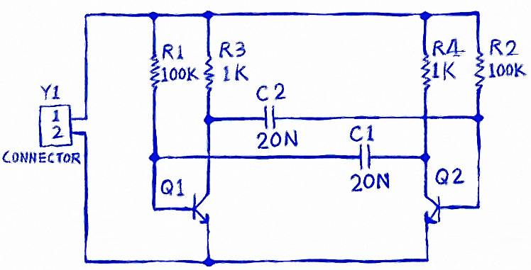
The design you will be capturing and designing a printed circuit board (PCB) for is a simple astable multivibrator. The circuit is shown below; it uses two general purpose NPN transistors configured as a self-running astable multivibrator.
You're ready to begin capturing (drawing) the schematic. The first step is to create a PCB project.
Creating a New PCB Project
In Altium's software, a PCB project is the set of design documents (files) required to specify and manufacture a printed circuit board. The project file, for example, Multivibrator.PrjPCB, is an ASCII text file that lists the documents that are in the project as well as other project-level settings, such as the required electrical rule checks, project preferences, and project outputs, such as print and CAM settings.
A new project is created in the Create New Project From Template dialog.

Adding a Schematic to the Project
The next step is to add a new schematic sheet to the project.

Setting the Document Options
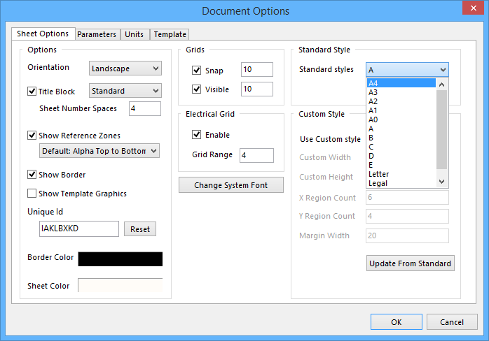
Before you start drawing your circuit, it is worth setting up the appropriate document options, including the sheet size and the Snap and Visible grids.
Components and Libraries in CircuitStudio
Related article: Component Management in CircuitStudio
The real-world component that gets mounted on the board is represented as a schematic symbol during design capture, and as a PCB footprint for board design. CircuitStudio components can be stored in local libraries or they can be placed directly from the Altium Content Vault, which is a globally-accessible component storage system that contains thousands of components, each with a symbol, footprint, component parameters, and links to suppliers.
The following component storage options can be used in CircuitStudio:
| Library Type | Function |
|---|---|
| Schematic Library | Schematic component symbols are created in schematic libraries (*.SchLib). Each symbol can become a component by adding links to a PCB footprint and adding component parameters to detail the component's specifications. |
| PCB Library | PCB footprints (models) are stored in PCB libraries (*.PcbLib). The footprint includes the electrical elements, such as the pads, as well as the mechanical elements, such as the component overlay, dimensions, glue dots, etc. It also can include a 3D definition, which is created by placing 3D Body objects or by importing a STEP model. |
| Library Package / Integrated Library | As well as working directly from the schematic and PCB libraries, you can also compile the component elements into an integrated library (*.IntLib). Doing this results in a single, portable library that holds all the models and symbols. An integrated library is compiled from a Library package (*.LibPkg), which is essentially a special-purpose project file with the source schematic (*.SchLib) and PCB libraries (*.PcbLib) added to it as source documents. As part of the compilation process, you can also check for potential problems, such as missing models and mismatches between schematic pins and PCB pads. |
| Altium Content Vault | The Content Vault is much more than a library. Components stored in the cloud, accessible from anywhere with internet access. Content Vault components include: symbol, footprint(s), component parameters, and links to suppliers. They are organized into folders - by manufacturer or by package type for generics. |
Accessing Components
Components are accessed through either:
- the Libraries panel (View | System | Libraries) for library components, or
- the Vaults panel (File » Vault Explorer) for Content Vault components.

Access components through either the Libraries pane, or the Vaults panel.
Making Libraries Available to Access the Components
In CircuitStudio, library-based components can be placed from Available Libraries. The libraries that are available include:
- Libraries in the current project - if a library is part of the project, the components in it are automatically available for placement within that project.
- Installed libraries - these are libraries that have been installed in CircuitStudio and their components are available for use in any open project.
Libraries are installed on the Installed tab of the Available Libraries dialog. To open the dialog, click the Libraries button at the top of the Libraries panel. If the panel is not currently visible, click View | System | Libraries to display it.
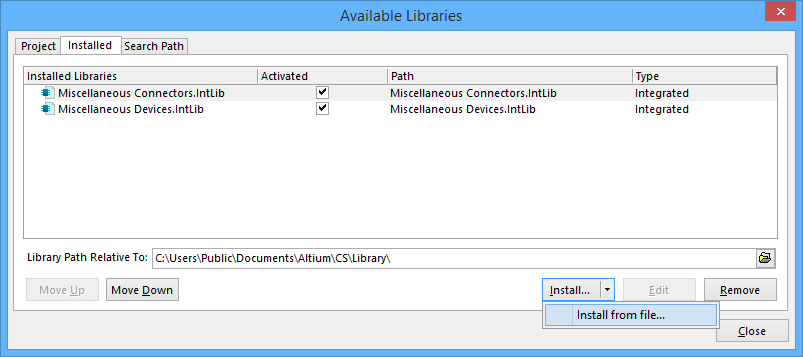
Install the required libraries to make their components available for designs.
Finding a Component in Libraries
To help you find the component you need, CircuitStudio includes powerful library searching capabilities. Although there are components that are suitable for the multivibrator design available in the pre-installed libraries, it is useful to know how to use the search feature to find components.
The Libraries Search dialog is accessed by clicking the Search button on the Libraries panel. The upper half of the dialog is used to define what you are searching for, the lower half is used to define where to search. The search can be in the libraries that are already installed (Available libraries) or it can be in libraries located on the hard drive (Libraries on path).
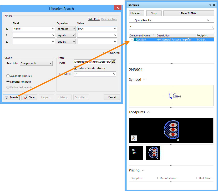
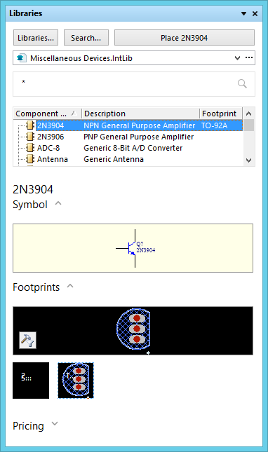
If you were working from libraries, the first step would be to search for a suitable general-purpose NPN transistor, such as a 2N3904.
Locating a Component in an Available Library
Libraries that are already installed are listed in the drop-down at the top of the panel. Click to select a library and display the components stored in it. Select the Miscellaneous Devices. IntLib library from the list, then use the component Filter in the panel to locate the required 2N3904 component within the library. Since the Miscellaneous Devices library is already installed, this component is ready to place. Do not place it though; instead you will use a transistor from the Altium Content Vault.

Making the Content Vault Available to Access Components
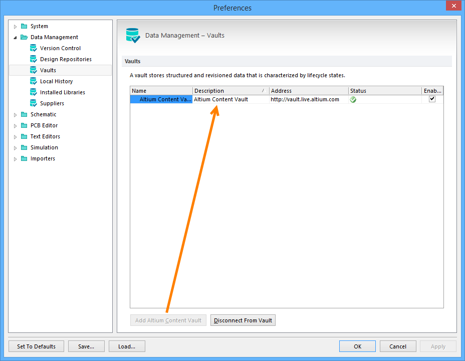
The Altium Content Vault is completely separate from the installed CircuitStudio software. To access the components in the Content Vault, you must first connect to it. This is done by clicking the Add Altium Content Vault button in the Data Management - Vaults page of the Preferences dialog.
Finding a Component in the Content Vault
Related article: Vaults panel
Once you have connected to the Altium Content Vault, you can explore or search for a component. This is done in the Vaults panel by selecting File » Vault Explorer to display the panel. The panel includes a powerful search feature. Enter the search string into the search field at the top-right of the panel.
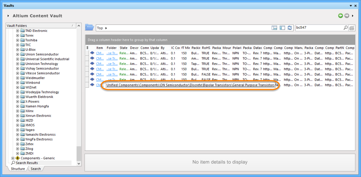
Searching for the general-purpose transistor BC547 in the Altium Content Vault. Each result is a hyperlink. Hover for more information and click to examine.
Working in the Vaults Panel
The Vaults panel includes a number of sections that can be resized as required. Take some time to explore the features and behavior of the panel; right-click for context-specific commands.
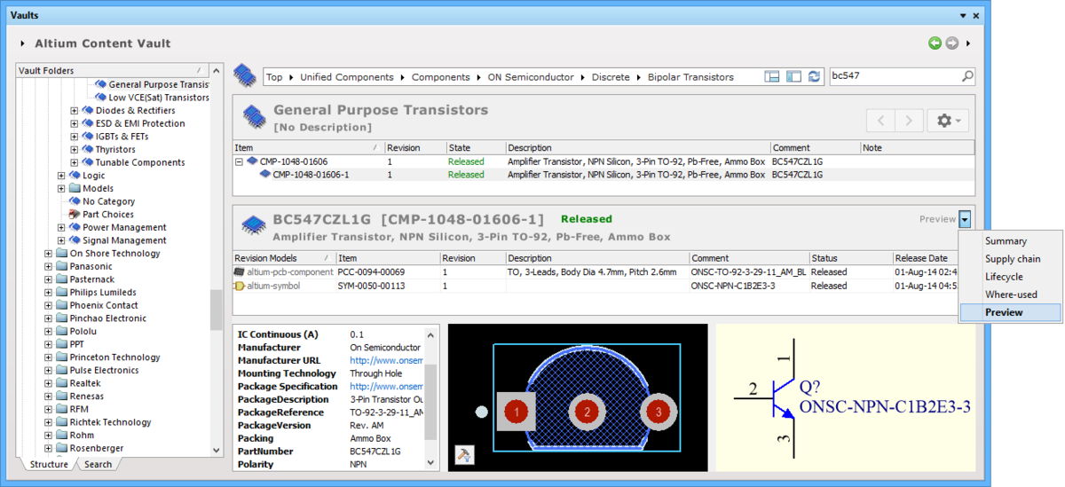
Use the Preview mode to examine the models and parameters included with the selected component.
- Components are organized in folders. Use the Vaults Folders section on the left of the panel to browse.
- There are a large number of components stored in the Altium Content Vault, therefore, it can be more efficient to search as just described.
- Search results are presented as a series of links; click on a link to examine a component in detail; use the Back button at the top right of the panel to return to the search results.
- Clicking on a specific component in the search results displays only that component in the folder in which it is stored. Select Refresh All from the menu at the top left of the panel to display all components in that folder.
- The lower region of the panel has a number of display modes, including: Summary, Supply Chain, Lifecycle, Where-used, and Preview. Use the arrow icon to select the required mode, as shown in the image above.
Placing Components on the Schematic
Components are placed onto the current schematic sheet from the Libraries or Vaults panel. This can be done by:
From the Libraries Panel
- Clicking the Place button - the component appears floating on the cursor; position it then click to place.
- Double-clicking - double-click the component in the list of components in the panel. The component appears floating on the cursor; position it then click to place.
- Click and drag - click and drag the component onto the sheet. This mode requires that the mouse button is held down; the component is placed when the mouse button is released.
From the Vaults Panel
- Right-click on the component then select Place <component>. The component appears floating on the cursor; position it then click to place. Note that if the Vaults panel is floating over the workspace, it will fade to allow you to see the schematic and place the component.
- Click and drag - click and drag the component from the Vaults panel and drop it onto the schematic. This mode requires that the mouse button is held down; the component is placed when the mouse button is released.
Multivibrator Parts
The following components were searched for and used in the Multivibrator circuit.
| Designator | Description | Vault Item-Revision or Library Component Name | Comments |
|---|---|---|---|
| Q1, Q2 | General purpose NPN transistor, e.g., BC547 or 2N3904 | CMP-1048-01437-1 | searched Vault for BC547, chose the first one |
| R1, R2 | 100K resistor, 5%, 0805 | CMP-1013-00122-1 | searched Vault for 100K 5% 0805 |
| R3, R4 | 1K resistor, 5%, 0805 | CMP-1013-00074-1 | searched Vault for 1K 5% 0805, note that search also returns 1K3, 1K8, etc. |
| C1, C2 | 22nF capacitor, 10%, 16V, 0805 | CMP-1036-04042-1 | searched Vault for 22nF 16V 0805 |
| Y1 | 2-pin header, thruhole | Header 2 | searched Available Libraries for header, component found in Miscellaneous Connectors.IntLib |
Once you have placed the components, the schematic should look similar to this:

All components are placed, ready for wiring.
You have now placed all the components. Note that the components shown in the image above are spaced so that there is plenty of room to wire to each component pin. This is important because you cannot place a wire across the bottom of a pin to get to a pin beyond it. If you do, both pins will connect to the wire. If you need to move a component, click-and-hold the body of the component then drag the mouse to reposition it.
Wiring the Circuit
Wiring is the process of creating connectivity between the various components of your circuit. To wire your schematic, refer to the sketch of the circuit and the animation shown below.
Use the Wiring tool to wire up your circuit.
Nets and Net Labels
Each set of component pins that you have connected to each other now form what is referred to as a net. For example, one net includes the base of Q1, one pin of R1 and one pin of C1. Each net is automatically assigned a system-generated name, which is based on one of the component pins in that net.
To make it easy to identify important nets in the design, you can add Net Labels to assign names. For the multivibrator circuit, you will label the 12V and GND nets in the circuit.
Net Labels have been added to complete the schematic.
Setting Up Project Options
Project-specific settings are configured in the Options for PCB Project dialog, shown below (Home | Project » Options or Project | Content | Project Options). The project options include the error checking parameters, a connectivity matrix, Class Generator, the Comparator setup, ECO generation, output paths and netlist options, Multi-Channel naming formats, Default Print setups, Search Paths, and project-level Parameters. These settings are used when you compile the project.
Project outputs, such as assembly, fabrication outputs and reports, are set up from the Outputs tab of the Ribbon. These settings are also stored in the Project file so they are always available for this project. See Documentation Outputs for more information.
Checking the Electrical Properties of the Schematic
Schematic diagrams are more than just simple drawings - they contain electrical connectivity information about the circuit. You can use this connectivity awareness to verify your design. When you compile a project, the software checks for errors according to the rules set up in the Error Reporting and Connection Matrix tabs of the Options for Project dialog. When you compile the project, any violations that are detected will display in the Messages panel.
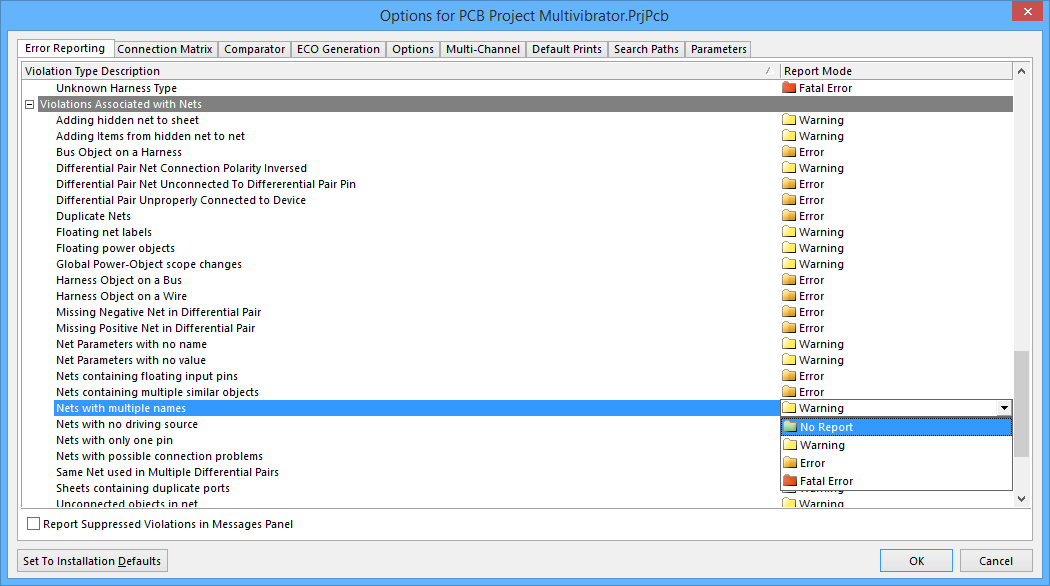
Setting up the Error Reporting
The Error Reporting tab in the Options for Project dialog is used to set up design drafting checks. The Report Mode settings show the level of severity of a violation. If you want to change a setting, click on a Report Mode next to the violation you want to change and choose the level of severity from the drop-down list. For this tutorial, we will use the default settings in this tab.
Setting Up the Connection Matrix
When the design is compiled, a list of the pins in each net is built in memory. The type of each pin is detected (e.g., input, output, passive, etc.,) then each net is checked to see if there are pin types that should not be connected to each other, for example, an output pin connected to another output pin. The Connection Matrix tab of the Options for Project dialog is where you configure which pin types are allowed to connect to each other. For example, look down the entries on the right side of the matrix diagram and find Output Pin. Read across this row of the matrix until you find the Open Collector Pin column. The square where they intersect is orange, indicating that an Output Pin connected to an Open Collector Pin on your schematic will generate an error condition when the project is compiled.
You can set each error type with a separate error level, e.g., from no report to a fatal error. Click on a colored square to change the setting; continue to click to move to the next check-level. Set the matrix so that Unconnected Passive Pin generates an Error, as shown in the image below.
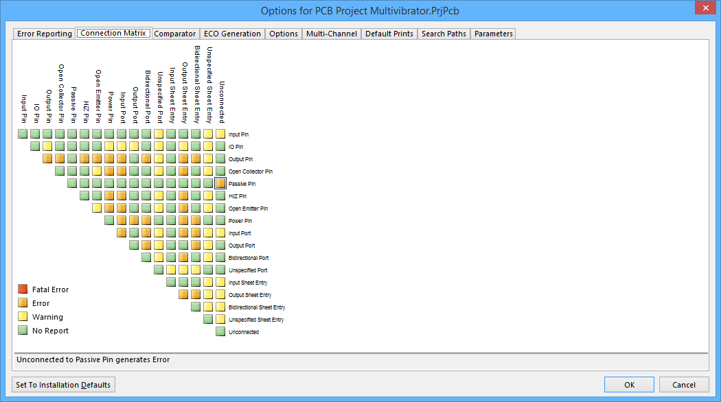
The Connection Matrix defines what electrical conditions are checked for on the schematic, note that the Unconnected - Passive Pin setting is being changed.
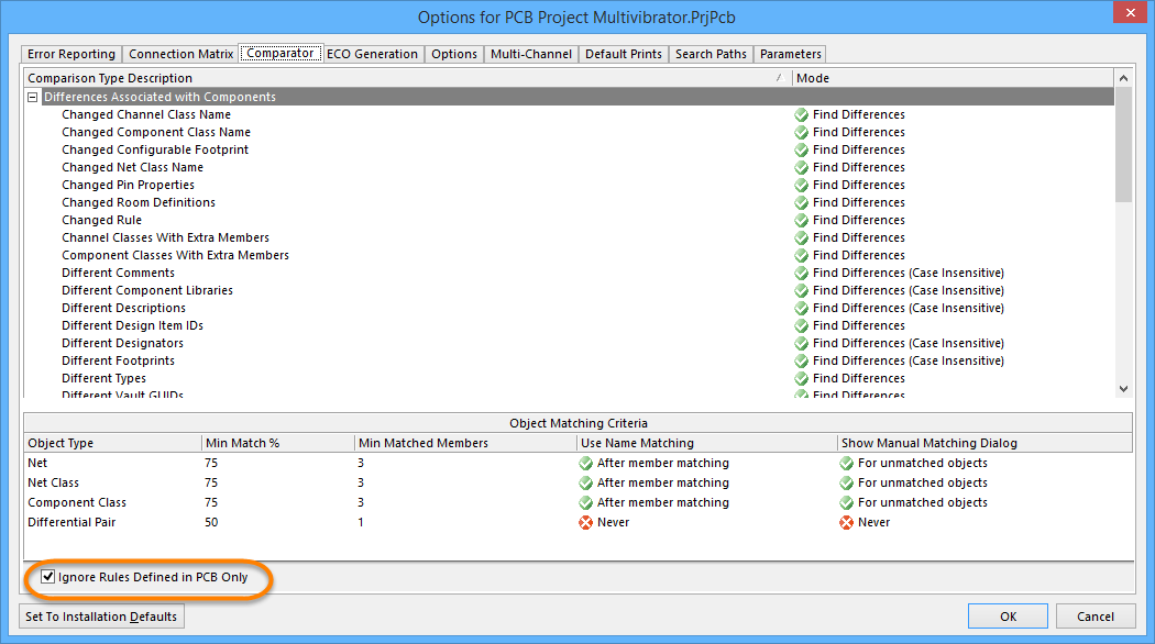
Setting Up the Comparator
The Comparator tab in the Options for Project dialog sets which differences between files will be reported or ignored when a project is compiled. Generally, the only time you will need to change settings in this tab is when you add extra detail to the PCB, such as design rules, and do not want those settings removed during design synchronization. If you need more detailed control, you can selectively control the comparator using the individual comparison settings.
For this tutorial, it is sufficient to confirm that the Ignore Rules Defined in PCB Only option is enabled.
Compiling the Project to Check for Errors
Compiling a project checks for drafting and electrical rules errors in the design documents and details all warnings and errors in the Messages panel. You have set up the rules in the Error Checking and Connection Matrix tabs of the Options for Project dialog and you are now ready to check the design.
To compile the project and check for errors, select Home | Project » Compile.
Use the Messages panel to locate and resolve design errors; double-click on an error to pan and zoom to that object.
Creating a New PCB
Before you transfer the design from the Schematic Editor to the PCB Editor, you need to create the blank PCB, name it and save it as part of the project.
The blank PCB has been added to the project.
Configuring the Board Shape and Location
There are a number of attributes of this blank board that need to be changed before transferring the design from the schematic editor including:
| Task | Process |
|---|---|
| Setting the origin | The PCB editor has two origins, the Absolute Origin, which is the lower left of the workspace, and the user-definable Relative Origin, which is used to determine the current workspace location. A common approach is to set the Relative Origin to the lower-left corner of the board shape. The Origin is set in the Grids and Units section of the Home tab on the Ribbon. |
| Change from Imperial to Metric units | The current workspace units are displayed on the Status bar, which is displayed at the bottom left of the workspace and also in the Grids and Units section of the Home tab on the Ribbon. For this tutorial, metric units will be used; to change the units, either press Q on the keyboard to toggle back and forth between Imperial and Metric units or click the |
| Selecting a suitable snap grid | You may have noticed that the current snap grid is 0.127mm, which is the old 10mil imperial snap grid, converted to metric. To change the snap grid at any time, select or type a new value in the Snap Grid setting in the Home | Grids and Units section of the Ribbon. Since you are about to define the overall size of the board, a very coarse grid can be used; enter a value of |
| Redefining the board shape to the required size | The board shape is shown by the black region with a grid in it. The default size for a new board is 4x4 inches; the tutorial board is 30mm x 30mm. Details for the process of defining a new shape for the board are outlined below. |
| Configuring the layers used in the design | As well as the copper, or electrical layers, on which you route, there are also general purpose mechanical layers, and special-purpose layers such as the component overlays (silkscreens), solder mask, paste mask, etc. The electrical and other layers will be configured shortly. |
Transferring the Design
The process of transferring a design from the capture stage to the board layout stage is launched using the Update command (Home | Project | Project » Update PCB Document Multivibrator.CSPcbDoc) on the schematic editor Ribbon (or Home | Project | Project » Import Changes from Multivibrator.PrjPcb from the PCB editor Ribbon).
When you run this command, the design is compiled and a set of Engineering Change Orders is created that:
- Lists all components used in the design and the footprint required for each. When the ECOs are executed, the software will attempt to locate each footprint in the currently available libraries or available Content Vault, and place each into the PCB workspace. If the footprint is not available, an error will occur.
- A list of all nets (connected component pins) in the design is created. When the ECOs are executed, the software will add each net to the PCB then attempt to add the pins that belong to each net. If a pin cannot be added, an error will occur - this most often happens when the footprint was not found or the pads on the footprint do not map to the pins on the symbol.
- Addition design data is then transferred, such as net and component classes.
Setting Up the PCB Workspace
Once all of the ECOs have been executed, the components and nets will appear in the PCB workspace to the right of the board outline.
Before we start positioning the components on the board, we need to configure certain PCB workspace and board settings, such as the layers, grids and design rules.
Configuring the Display of Layers
As well as the the layers used to fabricate the board including: signal, power plane, mask and silkscreen layers, the PCB Editor also supports numerous other non-electrical layers. The layers are often grouped in the following way:
- Electrical layers - includes the 32 signal layers and 16 internal power plane layers.
- Mechanical layers - there are 32 general purpose mechanical layers, which are used for design tasks such as dimensions, fabrication details, assembly instructions, or special purpose tasks, such as glue dot layers. These layers can be selectively included in print and Gerber output generation. They can also be paired, meaning that objects placed on one of the paired layers in the library editor will flip to the other layer in the pair when the component is flipped to the bottom side of the board.
- Special layers - these include the top and bottom silkscreen layers, the solder and paste mask layers, drill layers, the Keep-Out layer (used to define the electrical boundaries), the multilayer (used for multilayer pads and vias), the connection layer, DRC error layer, grid layers, hole layers, and other display-type layers.
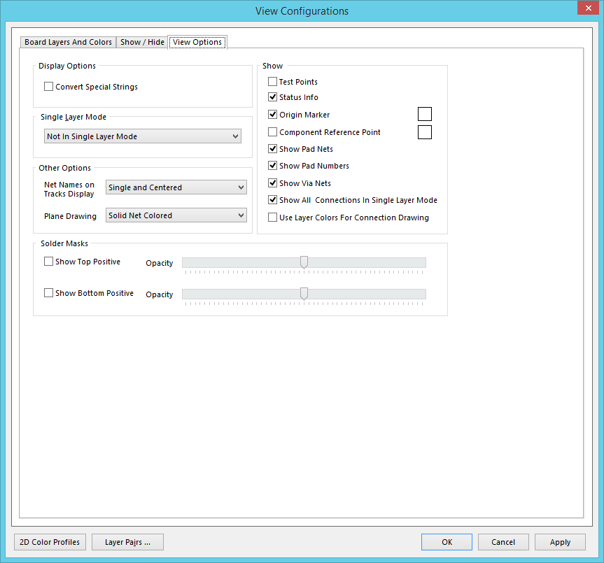
The display attributes of all layers are configured in the View Configurations dialog. To open the dialog:
- Select View | View | Switch to 3D » View Configurations » View Configuration or
- Click the current layer icon at the bottom-left of the workspace.
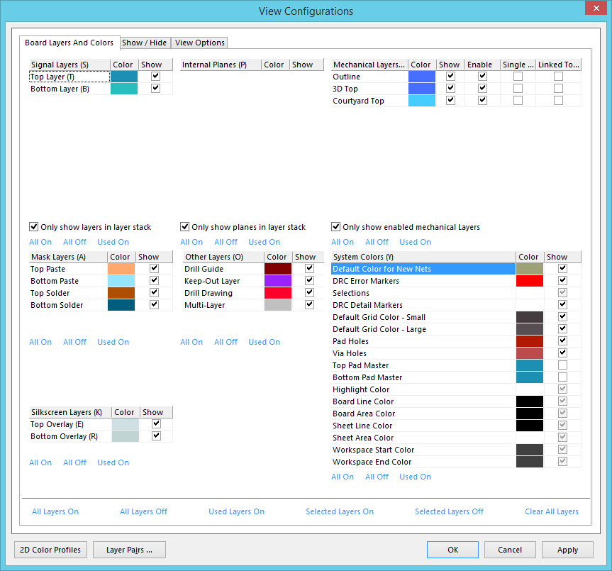
As well as the layer display state and color settings, the View Configurations dialog also gives access to other display settings including:
- How each type of object is displayed (solid, draft or hidden)oin the Show/Hide tab of the dialog.
- Various view options, such as if Pad Net names and Pad Numbers are to be displayed, the Origin Marker, if Special Strings should be converted, etc. These are configured on the View Options tab of the dialog.
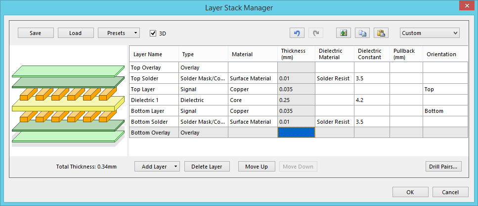
Physical Layers and the Layer Stack Manager
As well as the signal and power plane (solid copper) layers, the PCB Editor includes soldermask and silkscreen physical layers - these are all fabricated to make the physical board. The arrangement of these layers is referred to as the Layer Stack. The layer stack is configured in the Layer Stack Manager. Click Home | Board | Layer Stack Manager to open the dialog.
The Layer Stack Manager dialog is used to:
- Add/remove signal and power plane layers.
- Add/remove dielectric layers.
- Change the order of the layers.
- Configure the Material type for non-copper layers.
- Set the layer Thickness, Dielectric Material and Dielectric Constant.
- Define the Pullback amount (clearance from plane edge to board edge) for plane layers.
- Define the component orientation for that layer (advanced feature available in certain Altium products).
The tutorial PCB is a simple design and can be routed as a single-sided or double-sided board. The layer thicknesses shown below have been edited to use sensible metric values.
Imperial or Metric Grid?
The next step is to select a grid that is suitable placing and routing the components. All the objects placed in the PCB workspace are placed on the current snap grid.
Traditionally, the grid was selected to suit the component pin pitch and the routing technology that you planned to use for the board - i.e. how wide do the tracks need to be and what clearance is needed between tracks. The basic idea is to have both the tracks and clearances as wide as possible to lower the costs and improve the reliability. Ultimately, the selection of track/clearance is driven by what can be achieved on each design, which comes down to how tightly the components and routing must be packed to get the board placed and routed.
Over time, components and their pins have dramatically shrunk in size, as has the spacing of their pins. The component dimensions and spacing of their pins has moved from being predominantly imperial with thru-hole pins to being more-often metric dimensions with surface mount pins. If you are starting out a new board design, unless there is a strong reason, such as designed a replacement board to fit into an existing (imperial) product, you are better off working in metric.
Why?
Because the older, imperial components have big pins with lots of room between them. On the other hand, the small, surface mount devices are built using metric measurements - they are the ones that need a high level of accuracy to ensure that the fabricated/assembled/functional product works and is reliable. Also, the PCB editor can easily handle routing to off-grid pins, so working with imperial components is not onerous.
Suitable Grid Settings
For a design such as this simple tutorial circuit, practical grid and design rule settings would be:
| Setting | Value | Where |
|---|---|---|
| Routing width | 0.25 mm | Routing Width design rule |
| Clearance | 0.25 mm | Electrical Clearance design rule |
| Board definition grid | 5 mm | Cartesian Grid Editor |
| Component placement grid | 1 mm | Cartesian Grid Editor |
| Routing grid | 0.25 mm | Cartesian Grid Editor |
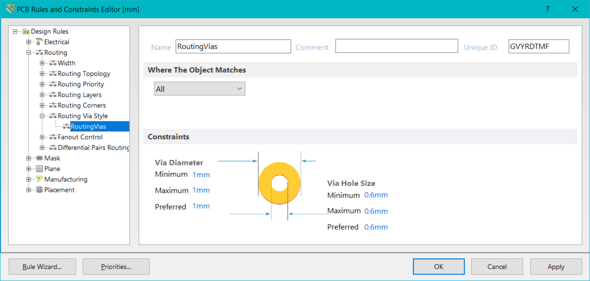
| Via size | 1 mm | Routing Via Style design rule |
| Via hole | 0.6 mm | Routing Via Style design rule |
This routing grid is chosen not just to allow tracks to be placed as close as possible and still satisfy the clearance; the PCB editor manages this automatically. The point of setting the grid to be equal to, or a fraction of, the track+clearance is not just to ensure that the clearance is maintained, it is to ensure tracks are placed so that they do not waste potential routing space, which can easily happen if a very fine grid is used.
Setting the Snap Grid
The value of the snap grid can be configured directly in the Home tab of the Ribbon, or it can be configured in the Cartesian Grid Editor dialog (Home | Grids and Units | Properties).
Set the Snap Grid to 1 mm, ready to position the components.
Setting Up the Design Rules
Main article: PCB Design Rules References
The PCB Editor is a rules-driven environment, meaning that as you perform actions that change the design, such as placing tracks, moving components, or autorouting the board, the software monitors each action and checks to see if the design still complies with the design rules. If it does not, the error is immediately highlighted as a violation. Setting up the design rules before you start working on the board allows you to remain focused on the task of designing, confident in the knowledge that any design errors will immediately be flagged for your attention.
Design rules are configured in the PCB Rules and Constraints Editor dialog as shown below (Home | Design Rules | Design Rules). The rules fall into 6 categories, which can then be further divided into design rule types. The rules cover electrical, routing, mask, plane, manufacturing, and placement requirements.
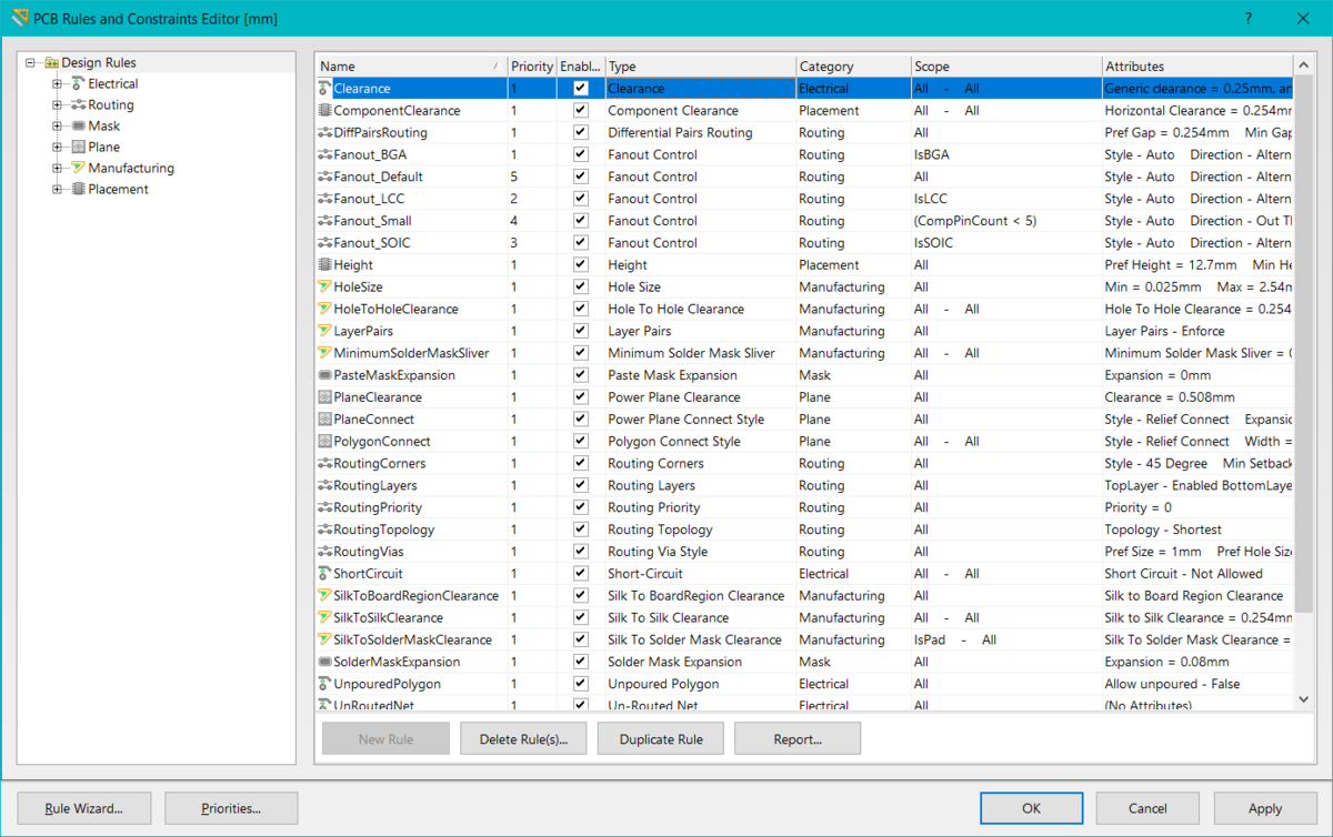
Routing Width Design Rules
The tutorial design includes a number of signal nets and two power nets. The default routing width rule (rule scope of All) will be configured at 0.25mm for the signal nets, and two more rules will be added to target the power nets.
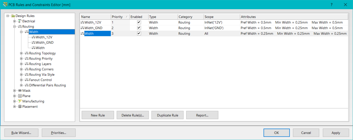
Three Routing Width design rules have been defined: the lowest priority rule targets All nets, the two higher priority rules target the 12V and GND nets.
Defining the Electrical Clearance Constraint
The next step is to define how close electrical objects that belong to different nets can be to each other. This requirement is handled by the Electrical Clearance Constraint. For the tutorial, a clearance of 0.25mm between all objects is suitable. Note that entering a value into the Minimum Clearance field will automatically apply that value to all of the fields in the grid region at the bottom of the dialog. You only need to edit in the grid region when you need to define a clearance based on the object-type.
![]()
Defining the Routing Via Style
If you place a via from the Ribbon, its values are defined by the built-in default primitive settings. As you route and change layers, a via is automatically added. In this situation, the via properties are defined by the applicable Routing Via Style design rule.
Existing Design Rule Violation
You might have noticed that the transistor pads are showing that there is a violation. Right-click over a violation and select Violations in the right-click menu. The details show that there is a:
- Clearance Constraint violation
- Between a Pad on the MultiLayer, and a Pad on the MultiLayer
- Where the clearance is 0.22mm, which is less than the specified 0.25mm
![]()
Positioning the Components on the PCB
There is a saying that PCB design is 90% placement and 10% routing. While you could argue about the percentage of each, it is generally accepted that good component placement is critical for good board design. Keep in mind that you may need to tune the placement as you route too.
Component Positioning and Placement options
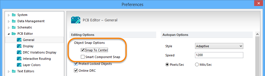
The default behavior when moving a component is to hold it by the reference point (Snap To Center) option defined in the PCB Library editor, rather than where you happened to click on it. The Smart Component Snap option allows you to override this behavior and snap to the nearest component pad, which is handy when you need to position a specific pad in a specific location.
Positioning Components
You can now position the components in suitable locations on the board.
To move a component either:
- Click and Hold the left mouse button on the component, move it to the required location, then release the mouse button to place it, or
- Run the Tools | Arrange | Move » Component command, then single-click to pick up a component, move it to the required location, then click once to place it. When you are finished, right-click to drop out of the Move Component command.
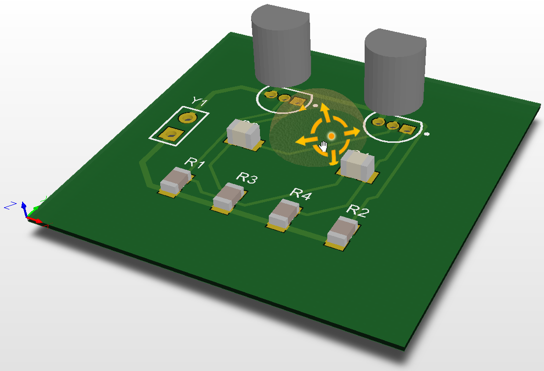
Components positioned on the board.
With everything positioned, it's time to do some routing!
Interactively Routing the Board
Routing is the process of laying tracks and vias on the board to connect the component pins. The PCB editor makes this job easy by providing sophisticated interactive routing tools, as well as the topological autorouter that optimally routes the whole or part of a board at the click of a button. While autorouting provides an easy and powerful way to route a board, there will be situations where you will need exact control over the placement of tracks. In these situations you can manually route part or all of your board.
In this section of the tutorial, you will manually route the entire board single-sided, with all tracks on the top layer. The Interactive Routing tools help maximize routing efficiency and flexibility in an intuitive way, including cursor guidance for track placement, single-click routing of the connection, pushing obstacles, and automatically following existing connections, all in accordance with applicable design rules.
Preparing for Interactive Routing
Before starting to route, it is important to configure the Interactive Routing options found in the PCB Editor - Interactive Routing page of the Preferences dialog.

Time to Route
- Interactive routing is launched by clicking the Route button - - on the Home tab (or press the Shortcut key R). You only need to use the drop-down menu if you need to select one of the other routing options.
- Since the components are mostly surface mount, the board will be routed on the top layer. As you place tracks on the top layer of the board, you use the ratsnest (connection lines) to guide you.
- Tracks on a PCB are made from a series of straight segments. Each time there is a change of direction, a new track segment begins. Also, by default, the PCB editor constrains tracks to a vertical, horizontal or 45° orientation, which allows you to easily produce professional results. This behavior can be customized to suit your needs; for this tutorial we will use the default.
- After reaching the target pad, right-click or press Esc to release that connection - you will remain in Interactive Routing mode, ready to click on the next connection line.
A simple animation showing the board being routed. Note that many of the connections are finished using the Ctrl+Click to autocomplete feature.
Routing Tips
Keep in mind the following points as you are routing:
| Keystroke | Behavior |
|---|---|
| ~ (tilda) or Shift+F1 | Pop up a menu of interactive shortcuts - most settings can be changed on the fly by pressing the appropriate shortcut or selecting from the menu. |
| * or Ctrl+Shift+WheelRoll | Switch to the next available signal layer. A via is automatically added in accordance with the applicable Routing Via Style design rule. |
| Shift+R | Cycle through the enabled conflict resolution modes. Enable the required modes on the PCB Editor - Interactive Routing Preferences page. |
| Shift+S | Toggle single layer mode on and off. This is ideal when there are many objects on multiple layers. |
| Spacebar | Toggle the current corner direction. |
| Shift+Spacebar | Cycle through the various track corner modes. The styles are: any angle, 45°, 45° with arc, 90°, and 90° with arc. There is an option to limit this to 45° and 90° on the PCB Editor - Interactive Routing Preferences page. |
| Ctrl+Left-Click | Auto-complete the connection being routed. Auto-complete will not succeed if there are unresolvable conflicts with obstacles. |
| Ctrl | Temporarily suspend the Hotspot Snap, or press Shift + E to cycle through the three available modes (off / on for current layer / on for all layers). |
| End | Redraw the screen. |
| PgUp / PgDn | Zoom in / out centered around the current cursor position. Alternatively, use the standard Windows mouse wheel zoom and pan shortcuts. |
| Backspace | Remove the last committed track segment. |
| Right-click or ESC | Drop the current connection, remaining in Interactive Routing mode. |
Interactive Routing Modes
The PCB editor's Interactive Routing engine supports a number of different modes, with each mode helping you to deal with particular situations. Press the Shift+R shortcut to cycle through these modes as you interactively route. Note that the current mode is displayed on the Status bar.
The available interactive routing modes include:
- Ignore - this mode lets you place tracks anywhere, including over existing objects, displaying but allowing potential violations.
- Stop at first obstacle - in this mode, the routing is essentially manual; as soon as an obstacle is encountered, the track segment will be clipped to avoid a violation.
- Push - this mode will attempt to move objects (tracks and vias) that are capable of being repositioned without violation to accommodate the new routing.
Modifying and Rerouting
To modify an existing route, there are two approaches: reroute or re-arrange.
Reroute an Existing Route
- There is no need to un-route a connection to redefine its path. Click the Route button and start routing the new path.
- The Loop Removal feature will automatically remove any redundant track segments (and vias) as soon as you close the loop and right-click to indicate you are complete (Loop Removal was enabled earlier in the tutorial).
- You can start and end the new route path at any point, swapping layers as required.
- You can also create temporary violations by switching to Ignore Obstacle mode (as shown in the animation below), which you later resolve.
A simple animation showing the Loop Removal feature being used to modify existing routing.
Re-arrange Existing Routes
- To interactively slide or drag track segments across the board, click, hold and drag as shown in the animation below.
- The PCB editor will automatically maintain the 45/90 degree angles with connected segments, shortening and lengthening them as required.
An animation showing track dragging being used to tidy up existing routing.
Track Dragging Tips
- During dragging, the routing conflict resolution modes also apply (Ignore, Push). Press Shift+R to cycle through the modes as you drag a track segment.
- Existing pads and vias will be jumped, or vias will be pushed if necessary and possible.
- To convert a 90 degree corner to a 45 degree route, start dragging on the corner vertex. If a chooser window pops up (as shown in the animation above), you can select either track segment.
- While dragging you can move the cursor and hotspot snap it to an existing, non-moving object such as a pad (shown above). Use this to help align the new segment location with an existing object and avoid very small segments being added.
- To break a single segment, select the segment first, then position the cursor over the center vertex to add in new segments (shown above).
- Change the default select-then-drag mode using the Unselected via/track and Selected via/track options on the PCB Editor - Interactive Routing page of the Preferences dialog.
Automatically Routing the Board
Configuring the Autorouter
CircuitStudio also includes a topological autorouter. A topological autorouter uses a different method of mapping the routing space - one that is not geometrically constrained. Rather than using workspace coordinate information as a frame of reference (dividing it into a grid), a topological autorouter builds a map using only the relative positions of the obstacles in the space, without reference to their coordinates.
Topological mapping is a spatial-analysis technique that triangulates the space between adjacent obstacles. This triangulated map is then used by the routing algorithms to "weave" between the obstacle pairs from the start route point to the end route point. The greatest strengths of this approach are that the map is shape independent (the obstacles and routing paths can be any shape) and the space can be traversed at any angle - the routing algorithms are not restricted to purely vertical or horizontal paths as with a rectilinear expansion routers.
Translating this into a user interface, the router has a number of different routing passes available, such as Fan Out to Plane, Main, Memory, Spread, Recorner, etc. These are bundled together to create a Routing Strategy, which you can then run on their board. There are a number of pre-defined strategies already available in the Routing Strategies dialog, and new ones are easily created using the Strategy Editor.
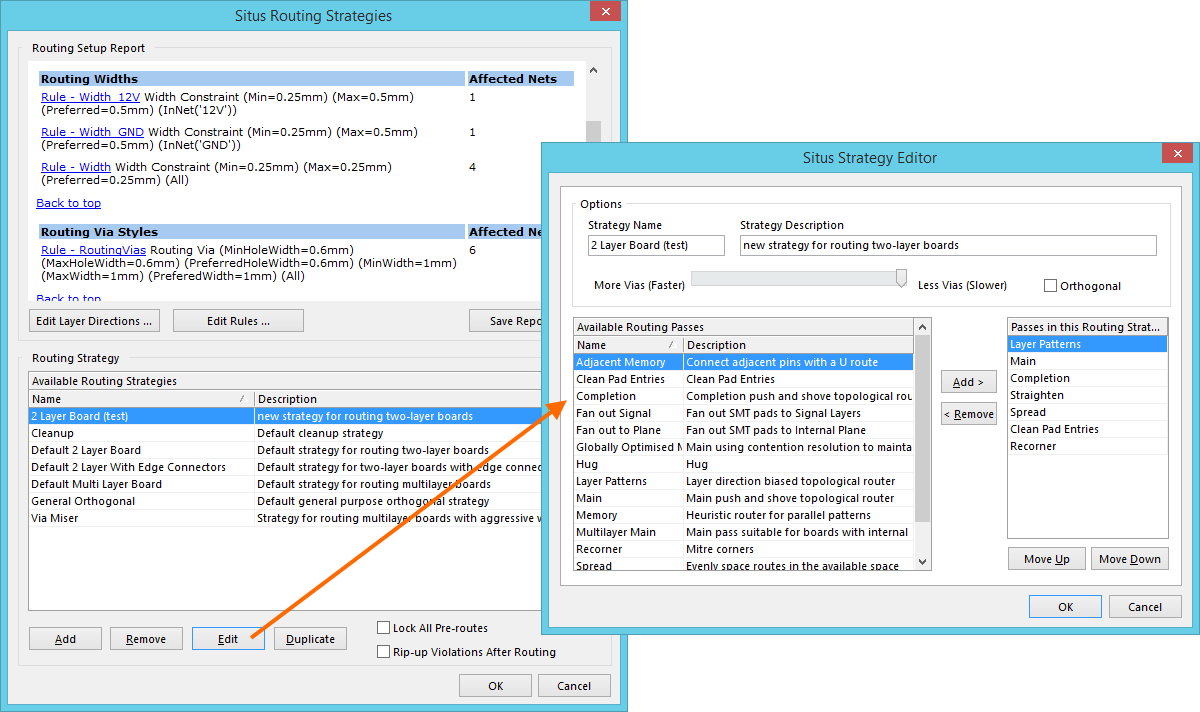
Select an existing routing strategy, or create a new one in the Strategy Editor.
Running the Autorouter
- The autorouter is configured and run from the Tools | Autoroute | Autoroute menu on the Ribbon. Selecting All from the menu opens the Routing Strategies dialog, which is used to configure the strategies, select the required strategy, and run the autorouter.
- The autorouter will route on the layers allowed by the Routing Layers design rule in the directions specified in the autorouter Layer Directions dialog (where possible).
The images below show the autorouting results using the Default two Layer Board Strategy on the left, and a user-defined strategy on the right (the chosen routing passes are shown in the image above).
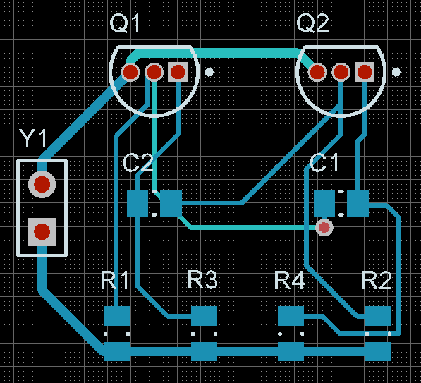
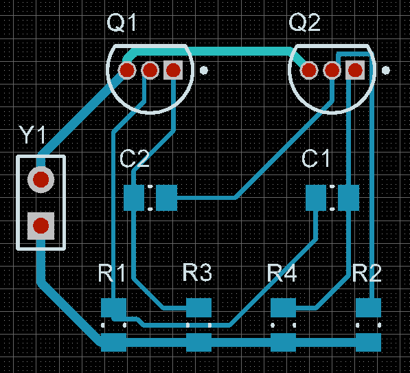
Autorouting results for the default two layer strategy (left image), and a user-defined strategy (right image).
Configuring the Display of Rule Violations
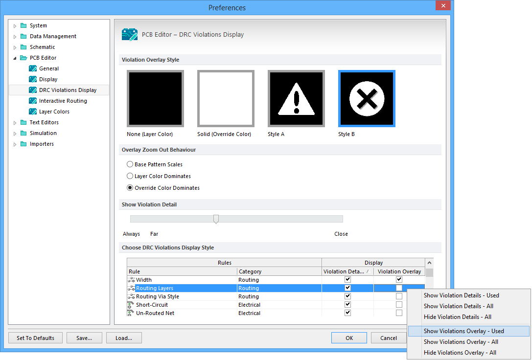
CircuitStudio has two techniques for displaying design rule violations, each with their own advantages. These are configured on the PCB Editor - DRC Violations Display page of the Preferences dialog:
- Violation Overlay - Violations are identifed by the primitive-in-error being highlighted in the color chosen for the DRC Error Markers (configured in the View Configurations dialog; press L to open). The default behavior is to show the primitives in a solid color when zoomed out, changing to the selected Violation Overlay Style as you zoom. The default is Style B, i.e. a circle with a cross in it.
- Violation Details - As you zoom further in, Violation Detail is added (if enabled) that details the nature of the error. Use the Show Violation Detail slider to define at what zoom level the Violation Details start to display. Enable the required Display options in the Preferences dialog.
Violations are shown in solid red (left image); as you zoom in, this changes to an Overlay (center image) and as you zoom in further, Violation Details are added.
Preparing to run a Design Rule Check (DRC):
- Open the View Configurations dialog (View|View |Switch to 3D » View Configurations » View Configuration). On the Board Layers And Colors tab, ensure the Show checkbox next to the DRC Error Markers option in the System Colors region is enabled (checked) so that DRC error markers will be displayed.
- Confirm that the Online DRC (Design Rule Checking) system is enabled on the PCB Editor - General page of the Preferences dialog. Keep the Preferences dialog open; switch to the PCB Editor - DRC Violations Display page of the dialog.
- The PCB Editor - DRC Violations Display page of the Preferences dialog is used to configure how violations are displayed in the workspace. There are two different methods available for displaying violations, each with their own strengths.
- For the tutorial, right-click in the Display area of the PCB Editor - DRC Violations Display page of the Preferences dialog then select Show Violation Details - Used; right-click again then select Show Violation Overlay - Used (shown in the image above).
- You are now ready to check the design for errors.
Configuring the Rule Checker
The design is checked for violations by running the Design Rule Checker. Click the Design Rule Check button - ![]() - on the Home tab of the Ribbon to open the dialog. Both online and batch DRC are configured in this dialog.
- on the Home tab of the Ribbon to open the dialog. Both online and batch DRC are configured in this dialog.
DRC Report Options
- By default, the dialog opens showing the DRC Report Options page selected in the tree on the left of the dialog (shown below).
- The right side of the dialog displays a list of general reporting options. For more information about the options, press F1 when the cursor is over the dialog (try a second time if it fails to load the first time). Leave these options at their defaults.

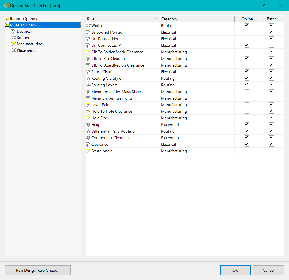
DRC Rules to Check
- The testing of specific rules is configured in the Rules to Check region of the dialog. Select this page in the tree on the left of the dialog to list all of the rule types (shown below). You can also examine them by type, for example, Electrical, by selecting that page on the left of the dialog.
- For most rule types, there are checkboxes for Online (check as you work) and Batch (check this rule when the Run Design Rule Check button is clicked).
- Click to enable/disable the rules as required. Alternatively, right-click to display the context menu. This menu allows you to quickly toggle the Online and Batch settings. Select the Batch DRC - Used On entry as shown in the image below.
Running a Design Rule Check (DRC)
When the Run Design Rule Check button at the bottom of the dialog is clicked, the DRC will run.
- The Messages panel will appear and list all detected errors.
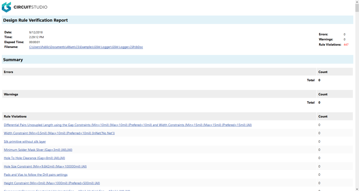
- If the Create Report File option was enabled in the Report Options page of the dialog, a Design Rule Verification Report will open in a separate document tab. A sample report is shown below.
- Below the summary of violating rules will be specific details about each violation.
- The links in the report are live. Click on an error to jump back to the board and examine that error on the board. Note that the zoom level for this click action is configured on the System - General Settings page of the Preferences dialog. You can experiment to find a zoom level that suits you.
Identifying the Error Condition
When you are new to the software, a long list of violations can initially seem overwhelming. A good approach to managing this is to disable and enable rules in the Design Rule Check dialog at different stages of the design process. It is not advisable to disable the design rules themselves, just the checking of them. For example, you would always disable the Un-Routed Net check until the board is fully routed.
- When a batch DRC is run on the tutorial board, there are four clearance constraint violations, which means the measured values are less than the minimum amounts specified in the applicable design rule(s). You now know how to locate those violations (click the link in the report file or double-click in the Messages panel), and using the Violation Details, you can understand the error condition.
- The image below shows the Violation Details for one of the clearance constraint errors, which is indicated by the white arrows and the
0.25mmtext. The next step is to work out what the actual value is so you know by how much it has failed.
The Violation Details show that the clearance between these two pads
is less that 0.25mm; it does not detail the actual clearance.
Apart from actually measuring the distance, there are two approaches to working out by how much the rule has failed:
- the right-click Violations submenu, or
- the PCB Rules and Violations panel.
The Violations Submenu
The right-click Violations submenu was described earlier in the Existing Design Rule Violation section.
- The image below shows how the Violations submenu details the measured condition against the value specified by the rule.
![]()
Right-click on a violation to examine what rule is being violated and the violation conditions.
The PCB Rules and Violations Panel
The second approach to understanding the error condition is to use the PCB Rules and Violations panel.
- Click the View | PCB | Rules and Violations button to display the panel.
- Click once on a Violation to jump to that violation; double-click on a violation to open the Violation Details dialog.
Resolving the Violation
As the designer, you have to work out the most appropriate way of resolving each design rule violation. There are two ways of resolving this clearance constraint:
- Decrease the size of the transistor footprint pads to increase the clearance between the pads, or
- Configure the rules to allow a smaller clearance between the transistor footprint pads.
Since the 0.25mm clearance is quite generous and the actual clearance is quite close to this value (0.22mm), a good choice in this situation would be to configure the rules to allow a smaller clearance. This can be done in the existing Clearance Constraint design rule, as shown below.
- The TH Pad - to - TH Pad value is changed to
0.22mmin the grid region of the rule constraint. To edit a cell first select it, then press F2. - This solution is acceptable in this situation because the only other component with thruhole pads is the connector, which has pads spaced over 1mm apart.
![]()
Well done! You have completed the PCB layout and are ready to produce output documentation. Before doing that, let's explore the PCB editor's 3D capabilities.
Viewing Your Board in 3D
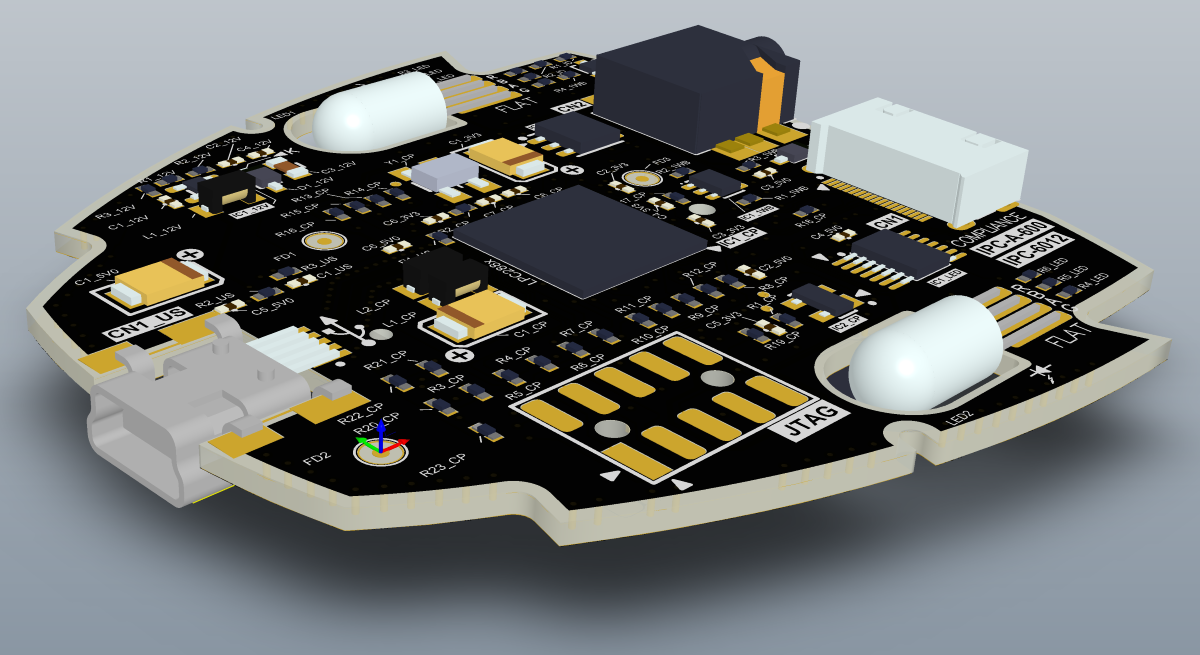
A powerful feature of CircuitStudio is the ability to view your board as a three-dimensional object. To switch to 3D, click the Switch to 3D button ![]() (View | View group), or press the 3 shortcut. The board will display as a three-dimensional object; the tutorial board is shown below.
(View | View group), or press the 3 shortcut. The board will display as a three-dimensional object; the tutorial board is shown below.
You can fluidly zoom the view, rotate it and even travel inside the board using the following controls:
- Zooming - Ctrl + Right-drag mouse, or Ctrl + Roll mouse-wheel, or the PgUp / PgDn keys.
- Panning - Right-drag mouse, or the standard Windows mouse-wheel controls.
- Rotation - Shift + Right-drag mouse. Note that when you press Shift, a directional sphere appears at the current cursor position as shown in the image below. Rotational movement of the model is made around the center of the sphere (position the cursor before pressing Shift to position the sphere) using the following controls. Move the mouse around to highlight and select each one:
- Right-drag sphere when the Center Dot is highlighted - rotate in any direction.
- Right-drag sphere when the Horizontal Arrow is highlighted - rotate the view about the Y-axis.
- Right-drag sphere when the Vertical Arrow is highlighted - rotate the view about the X-axis.
- Right-drag sphere when the Circle Segment is highlighted - rotate the view about the Z-plane.
Hold Shift to display the 3D view directional sphere, then click and drag the right-mouse button to rotate.
Tips for Working in 3D
- Press L to open the View Configurations dialog when the board is in 3D Layout Mode in which you can configure the 3D workspace display options. There are options to choose various surface and workspace colors, as well as vertical scaling, which is handy for examining the PCB internally. Some surfaces have an opacity setting - the greater the opacity, the less 'light' passes through the surface, which makes objects behind less visible. You can also choose to show 3D bodies or render 3D objects in their (2D) layer color.
- To display the components in 3D, each component needs to have a suitable 3D model.
- You can import a 3D STEP-format model into the component footprint in the Library editor; place a 3D Body Object then select the Generic STEP Model type to embed a STEP model inside that 3D Body Object.
- Check out 3D Content Central for STEP-format component models.
- If there is no suitable STEP model available, create your own component shape by placing multiple 3D Body Objects in the footprint in the Library editor.
Output Documentation
Now that you've completed the design and layout of the PCB, you're ready to produce the output documentation needed to get the board reviewed, fabricated and assembled.
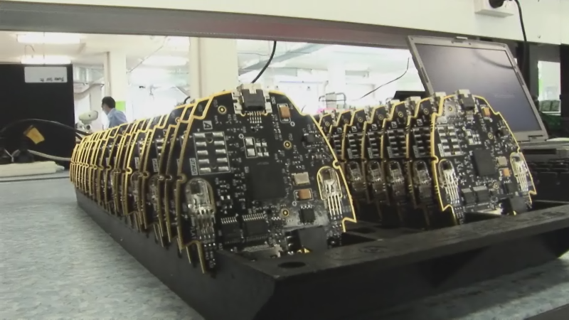
The ultimate objective is to fabricate and assemble the board.
Available Output Types
Because a variety of technologies and methods exist in PCB manufacture, CircuitStudio has the ability to produce numerous output types for different purposes:
Assembly Outputs
- Assembly Drawings - component positions and orientations for each side of the board.
- Pick and Place Files - used by robotic component placement machinery to place components onto the board.
Documentation Outputs
- Composite Drawings - the finished board assembly, including components and tracks.
- PCB 3D Prints - views of the board from a three-dimensional view perspective.
- Schematic Prints - schematic drawings used in the design.
Fabrication Outputs
- Composite Drill Drawings - drill positions and sizes (using symbols) for the board in one drawing.
- Drill Drawing/Guides - drill positions and sizes (using symbols) for the board in separate drawings.
- Final Artwork Prints - combines various fabrication outputs together as a single printable output.
- Gerber Files - creates manufacturing information in Gerber format.
- NC Drill Files - creates manufacturing information for use by numerically controlled drilling machines.
- ODB++ - creates manufacturing information in ODB++ database format.
- Power-Plane Prints - creates internal and split plane drawings.
- Solder/Paste Mask Prints - creates solder mask and paste mask drawings.
- IPC-2581 Standard - creates an XML-based single file format that incorporates a rich range of board fabrication data – from layer stackup details to full pad/routing /component information and the Bill Of Materials (BOM).
Report Outputs
- Bill of Materials - creates a list of parts and quantities (BOM), in various formats that are required to manufacture the board.
- Report Single Pin Nets- creates a report listing any nets that only have one connection.
- Electrical Rules Check - formatted report of the results of running an Electrical Rules Check.
Individual Outputs or Managed Output Generation
CircuitStudio has two separate mechanisms for configuring and generating output:
- Individually - the settings for each output type are stored in the Project file. You selectively generate that output when required using the options on the Outputs tab. These outputs are written to the folder specified in the Output Path setting on the Options tab of the Options for PCB Project dialog.
- Managed Release - all output settings are stored in a special file in the project folder. You then generate all enabled outputs in a single action using the Generate Output Files dialog. Using this approach gives you confidence that all the correct outputs were generated from the same version of the source schematic and PCB files. The dialog is accessed either from the Project | Project Actions | Generate Outputs button or the Home | Project | Project » Generate outputs menu entry. These outputs are written to a folder named
\Default Configuration. Once you have configured and enabled each required Outputer, click the Generate button in the dialog to generate the outputs in the\Default Configurationfolder.
Configuring the Gerber Files
- Gerber continues to be the most common form of data transfer between board design and board fabrication.
- Each Gerber file corresponds to one layer of the physical board - the component overlay, top signal layer, bottom signal layer, top solder mask layer, etc. It is advisable to consult with your board fabricator to confirm their requirements before supplying the output files required to fabricate your design.
- If the board has any holes, an NC Drill file must also be generated using the same units, resolution, and position on film settings.
- Gerber files are configured in the Gerber Setup dialog. If you intend to use the managed release approach, open the Gerber Setup dialog from the Generate Output Files dialog by clicking Configure associated with the Gerber Files entry.

Configuring the Bill of Materials
CircuitStudio includes a highly configurable BOM generation feature that can generate output in a variety of formats including: text, CSV, PDF, HTML, and Excel. Excel-format BOMs can also have a template applied using one of the pre-defined templates or one of your own.
- BoM output is configured in the Bill of Materials For Project dialog. If you intend to use the managed release approach, you open the Bill of Materials For Project dialog from the Generate Output Files dialog.
- On the left side of the dialog there is a list of every component attribute for all components in the design. Enable the checkbox for each attribute you want to include in the BOM and clear the checkbox for any attributes you want to remove.
- The default settings for the BOM is to cluster by like components. Clustering is achieved by adding component attributes to the Grouped Columns region of the dialog. Click and drag these attributes out of the Grouped Columns and drop them into the All Columns region if you prefer every component to be on its own row in the BOM.
- The main grid region of the dialog is the content that is written into the BoM. In this region you can click and drag to reorder the columns, click on a column heading to sort by that column, ctrl+click to sub-sort by that column, define value-based filters for a column using the small drop-down in each column header, and right-click to force the columns to fit the current dialog width.
- The BOM generator sources its information from the schematic. Enable the Include Parameters From PCB option to access PCB information, such as location and side of board (note that this feature can also be used to configure and generate a configurable pick and place file, if required).
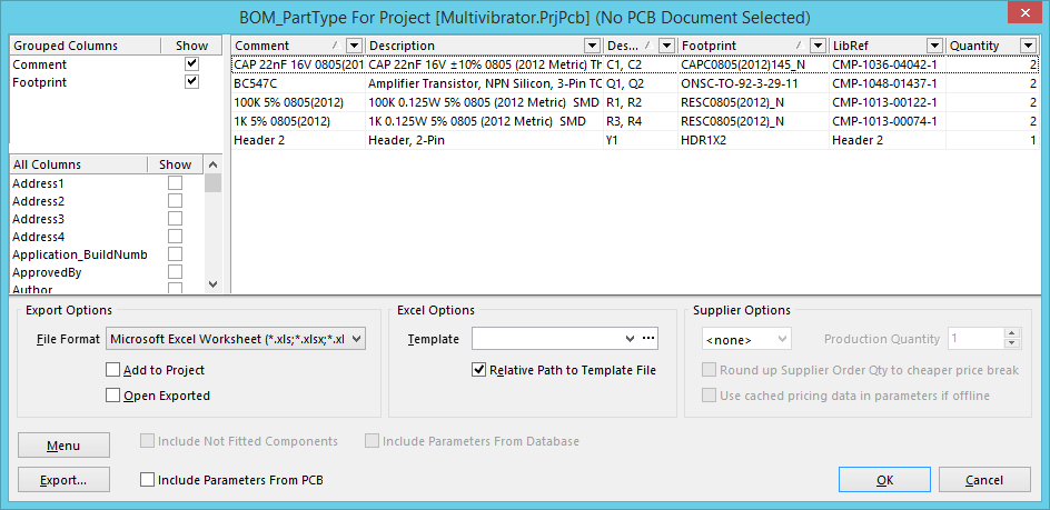
The default configuration for a new BoM is to group like components together.
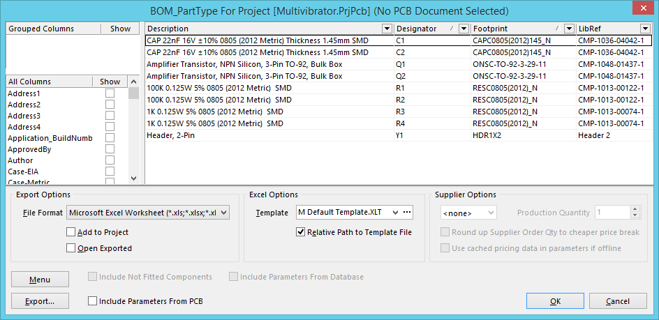
This BoM has been reconfigured to present each component as a unique entry.