
Component Pin Editor
Other Related Resources
Parent page: Sch Dialogs
The Component Pin Editor dialog
Summary
This dialog presents all pins for either the component in the active Schematic Library document, or a placed component (or part thereof) in the Schematic Editor. It provides a single, convenient location for you to modify certain properties of any pin associated to that component. In addition to providing a means of editing pin properties, the dialog allows you to add new pins or delete existing ones.
Access
The Component Pin Editor dialog is accessible from both the Schematic Editor and the Schematic Library Editor:
- Schematic Editor - double-click on the required placed component to access the Properties for Schematic Component dialog, then click the Edit Pins button at the bottom-left of the dialog.
- Schematic Library Editor - double-click on the component's entry in the Components region of the SCH Library panel to access the Library Component Properties dialog, then click the Edit Pins button at the bottom-left of the dialog.
Options/Controls
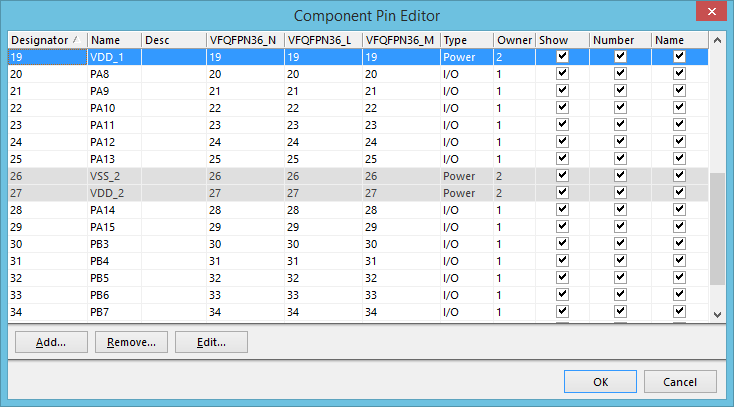
- Pin Grid - this area presents all pins for the component. For each pin, the following information is displayed:
- Designator - the numerical identifier of the pin. Each pin in a part must have a unique designator.
- Name - the display name for the pin. Note that while the pin name is optional, it is required when the pin is going to be hidden. A hidden pin is automatically connected to other hidden pins with the same name and to nets with the same name when a net-list is created. This entry corresponds to the Display Name property in the Pin Properties dialog.
- Desc - the description for the pin. This entry corresponds to the Description property in the Pin Properties dialog.
- Footprint Model Mapping - the pad of the indicated linked footprint model to which this pin of the schematic component is mapped. A separate field is presented for each linked footprint model.
- Type - the electrical type of the pin. The type is used when compiling a project or analyzing a schematic document to detect electrical connection errors (using the Electrical Rules Check feature). Available types are: Input, I/O, Output, Open Collector, Passive, HiZ, Open Emitter, and Power. This entry corresponds to the Electrical Type property in the Pin Properties dialog.
- Owner - the parent part to which the pin is associated. For a single-part component, this entry will always be 1. It is really only meaningful for a multi-part component. A multi-part component also includes a non-graphical part, Part Zero. Part Zero is used for pins that are to be included in all parts of the multi-part component, for example, power pins. This entry corresponds to the Part Number property in the Pin Properties dialog.
- Show - reflects whether the pin is visible on the sheet (enabled) or hidden (disabled). The power pins of multi-part components are typically hidden when their display would otherwise cause unnecessary clutter on the schematic sheet. This entry corresponds to the Hide property in the Pin Properties dialog.
- Number - this option is used to determine whether the designator for the pin is displayed (enabled) or hidden (disabled) when the parent part is placed on a schematic sheet. This entry corresponds to the Visible property (associated with the Designator field) in the Pin Properties dialog.
- Name - this option is used to determine whether the display name for the pin is displayed (enabled) or hidden (disabled) when the parent part is placed on a schematic sheet. This entry corresponds to the Visible property (associated with the Display Name field) in the Pin Properties dialog.
- Add - click this button to add a new pin to the component. The new pin will be assigned the next available designator (which can be pin 0) and will have the following default properties:
- Name - 0
- Desc - blank
- Mapping - all 0
- Type - Passive
- Owner - the number of the active/selected part.
- Show/Number/Name - all enabled.
- Remove - click this button to remove the currently selected pin from the component. A confirmation dialog will appear. Click Yes to proceed with the removal. If removing a pin from a placed component instance on a schematic, you may need to rewire any existing wiring that was connected to that pin.
- Edit - click this button to access the Pin Properties dialog for the currently selected pin entry in the grid in which all properties for the pin can be browsed and managed.
Right-click Menu
The Pins Grid right-click menu offers the following commands:
- Jump - use this command to jump to the currently selected pin within the workspace (zoomed and centered (where possible)).
- Add - use this command to add a new pin to the component (or part thereof).
- Remove - use this command to remove the currently selected pin from the component. A confirmation dialog will open. Click Yes to proceed with the removal.
- Edit - use this command to edit the currently selected pin using the Pin Properties dialog.
- Report - use this command to generate a report based on the information in the Pin Grid. The Report Preview dialog will open in which you can browse the report before printing or exporting into one of various supported formats.