Via
Contents
- Summary
- Availability
- Placement
- Auto-placement of Vias During Routing
- Default Settings versus Design Rules
- Graphical Editing
- Non-Graphical Editing
- Editing via an Associated Properties Dialog
- Editing via an Inspector Panel
- Working with Vias
- Thru-hole, Blind and Buried Vias
- Configuring the Layer Drill Pairs
- Solder Mask Expansions
- Testpoint Settings
- Configuring the Display of Vias
- Via Colors
- Vias and the Solder Mask
- Other Via Display Settings
Parent page: PCB Objects
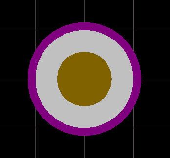
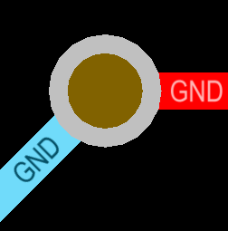
A via that spans and connects from the top layer (red) to the bottom layer (blue), and also connects to one
internal power plane (green).
Summary
A via is a primitive design object. It is used to form a vertical electrical connection between two or more electrical layers of a PCB. Vias are a three-dimensional object that has a barrel-shaped body in the Z-plane (vertical), with a flat ring on each (horizontal) copper layer. The barrel-shaped body of the via is formed when the board is drilled and through-plated during fabrication. In the X and Y planes, vias are circular like round pads. The key difference between a via and a pad is that as well as being able to span all layers of the board (top to bottom), a via can also span from a surface layer to an internal layer or between two internal layers.
Availability
Vias are available for placement in both the PCB editor and the PCB Library editors:
- PCB Editor - click Home | Place |
 from the main menus.
 - PCB Library Editor - click Home | Place | » Via from the main menus.
Placement
After launching the command, the cursor will change to a crosshair and you will enter via placement mode:
- Position the cursor then click or press Enter to place a via.
- Continue placing further vias, or right-click or press Esc to exit placement mode.
Auto-placement of Vias During Routing
When a net is being interactively routed, you can cycle through the available signal layers by pressing the * key on the numeric keypad. Alternatively, use the Ctrl+Shift+Roll Mouse Wheel combination to move through the signal layers. When this is done, the software will automatically place a via in accordance with the applicable Routing Via Style design rule. Note that multiple Via Style design rules can be defined, which allows different via sizes to be assigned to different nets.
Default Settings versus Design Rules
When a via is placed in free space, it is not possible for the software to apply a routing style design rule during placement. In this situation, the default via will be placed.
Graphical Editing
Vias cannot have their properties modified graphically, other than their location.
- To move a via and also move the connected tracks, click, hold and move the via. The connected routing will remain attached to the via as it is moved.
- To move a via without moving the connected tracks:
- In the PCB Editor - select the Tools | Arrange | Move » Move Object command, then click, hold and move the via.
- In the PCB Library Editor - select the Home | Arrange | Move » Move Object command, then click, hold and move the via.
Non-Graphical Editing
The following methods of non-graphical editing are available:
Editing via an Associated Properties Dialog
Dialog page: Via
This method of editing uses the following dialog to modify the properties of a via object.
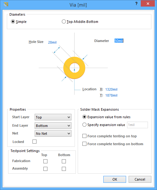
The Via dialog
The Via dialog can be accessed during placement by pressing the Tab key.
After placement, the dialog can be accessed in one of the following ways:
- Double-click on the placed via object.
- Place the cursor over the via object, right-click then choose Properties from the context menu.
Editing via an Inspector Panel
Panel pages: PCB Inspector, PCBLIB Inspector
An Inspector panel enables you to interrogate and edit the properties of one or more design objects in the active document. Used in conjunction with appropriate filtering, the panel can be used to make changes to multiple objects of the same kind, from one convenient location.
Working with Vias
Because vias are a key element of the routing, this section provides valuable information on working with them.
Thru-hole, Blind and Buried Vias
The default is for a via to span from the Top Layer through to the Bottom Layer; this is known as a thru-hole via. In a multilayer board, a via can also span other layers. The possible layers that a via can span depends on the fabrication technology used to fabricate the board. The traditional approach to manufacture a multi-layer board was to make it as a set of thin double-sided boards, which are then sandwiched together under heat and pressure to form a multi-layer board.
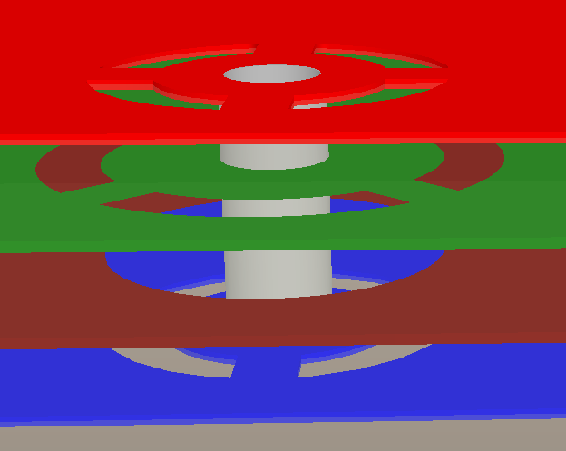
The image below shows a six layer board, as shown by the layer names at the left of the image. This board would first be fabricated as three double-sided boards (Top-Plane1, Mid1-Mid2, Plane2-Bottom), as indicated by the hatched core layers.
These double-sided boards can have via sites drilled if required, forming what are known as blind vias (via number 1) when the via spans from a surface layer to an inner layer; and buried vias when a via spans from one internal layer to another internal layer (via number 2). After the layers are pressed together into a single multi-layer board, thru-hole vias are drilled (via number 3).
The three types of vias that can be created, blind (1), buried (2) and thru-hole.
Another type of multi-layer board fabrication technology is call Build-up technology, where layers are added one after the other, often over a double-sided or traditional multi-layer board. When this technology is used, vias can be drilled with a laser after each layer is added during the build up process, resulting in a large number of possible layer-pairs that can be spanned. The layer-pairs used for each via are defined by the Start Layer and End Layer settings for the via.
Configuring the Layer Drill Pairs
When blind, buried or build-up type vias are to be used, the drill pairs must be configured. It is the presence of drill pairs that lets the software know that blind and/or buried vias are in use. This ensures that when the fabrication output files are generated from the completed board, there are suitable drill files for the various drill jobs that must be performed to create the blind or buried vias. Drill Pairs are configured in the Drill-Pair Manager dialog as shown in the image below. To open the dialog, first open the Layer Stack Manager dialog (click Home | Board | ![]() ), then click the Drill Pairs button to open the Drill-Pair Manager dialog.
), then click the Drill Pairs button to open the Drill-Pair Manager dialog.
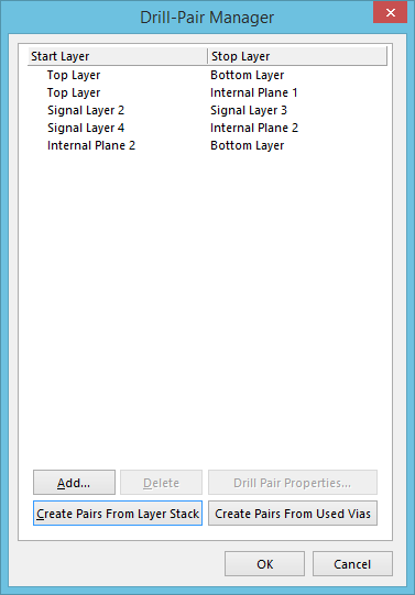
The arrangement of the copper layers is defined in the Layer Stack Manager.
From there, the Drill-Pair Manager can be opened to define the required drill pairs.
Solder Mask Expansions
An opening in the solder mask is automatically created by the software and is the same shape as the via. This opening can be larger (a positive expansion value) or smaller (a negative expansion value) than the via itself as defined by the Mask Expansion settings. The expansion is measured from the outer edge of the copper. Solder mask openings over a via can be slightly larger than the via copper area, they can be smaller to cover the copper area but not the drill hole, or they can be completely closed, which is called tented. The default is for the via to use the Expansion value from the Solder Mask Expansion rule. This can be overridden and local values can be defined directly in the Via dialog, if required.
The term tenting means to close off. If a tenting option is enabled, the settings in the applicable Solder Mask Expansion design rule will be overridden, resulting in no opening in the solder mask on that solder mask layer for this via. When this option is enabled, the Expansion value from rules and the Specify expansion value options are ignored.
Testpoint Settings
Use the Testpoint Settings to define this via as a testpoint for Fabrication and/or Assembly. A testpoint is a location where a test probe can make contact with the PCB to check for correct function of the board. Any pad or via can be nominated as a testpoint.
Configuring the Display of Vias
There are a number of display features available to help you work with vias.
Via Colors
The copper ring of the via is shown in the current Multi-Layer color. The via hole is shown in the current Via Holes color. Press the L shortcut when viewing the board in 2D to open the Board Layers and Colors tab of the View Configurations dialog. From here you can change the color assigned to Via Holes (in the System Colors region), or disable the display of holes.
A thru-hole via on the left. The via on the right is a blind via; the hole is shown in the start and end layer colors.
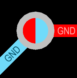
Vias and the Solder Mask
The default presentation of layers in the PCB editor is to always show the Multi-Layer as the top most layer. That can make it difficult to accurately view the contents of the solder mask layers, especially when a pad or via uses a negative mask expansion since the solder mask layer contents will disappear under the multi-layer object.
There are two options that can be changed to help with this:
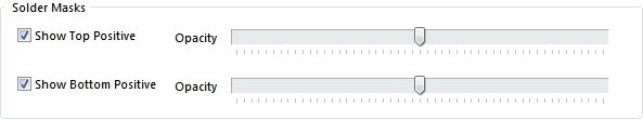
- Display the Solder Masks in the Positive and change their Opacity - the solder masks can be shown in the positive and be made semi-transparent using the Solder Masks options on the View Options tab of the View Configurations dialog, as shown below.
- Change the layer drawing order - set the
Current Layerto be drawn as the top-most layer in the Layer Drawing Order dialog. The dialog is accessed via the PCB Editor — Display page of the Preferences dialog (select File » System Preferences to open the Preferences dialog). Click on the Top Solder tab at the bottom of the workspace to make it the current layer.
By setting the Solder Mask to be positive and semi-transparent and changing the layer drawing order to show the Current Layer on top, when you make the Top Solder the current layer, the mask openings are accurately presented, as shown in the image below. The green arrows show the size of the solder mask opening for a via on the left, a pad where the mask opening is contracted in the center, and a pad where the opening is expanded on the right.
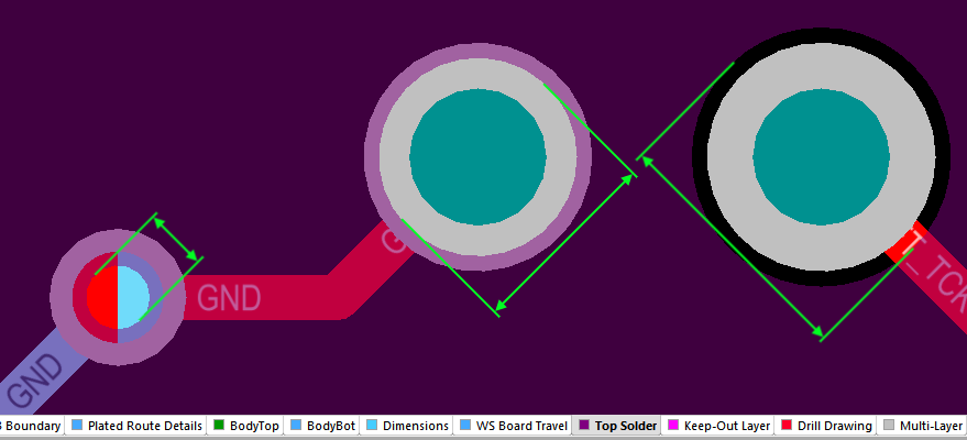
Configure the display settings to be able to examine the solder mask openings.
Other Via Display Settings
To display the via net name, enable the Show Via Nets option on the View Options tab of the View Configurations dialog.