Layer Stack Manager
Contents
Other Related Resources
Parent page: PCB Dialogs
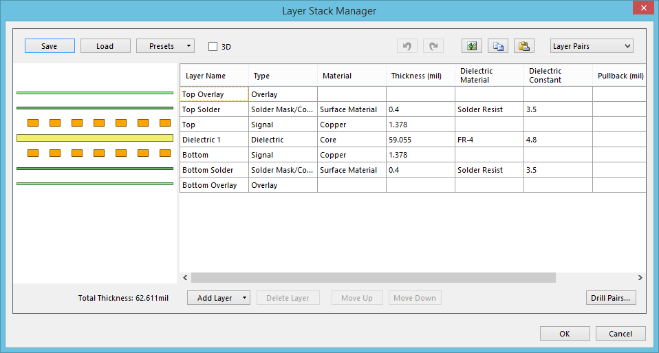
The Layer Stack Manager dialog
Summary
This dialog provides controls to configure and fully define the Layer Stack for the board design. The layer stack comprises all of the layers that are used in the overall PCB design. A variety of types of layers can be included in the layer stack including copper, dielectric, surface finish, and mask layers. Each layer must be completely specified in terms of its material and mechanical requirements including the material used, the thickness, the dielectric constant, and so on. The selection of materials and their properties should always be done in consultation with the board fabricator.
Access
The dialog is accessed from the PCB Editor by clicking Home | Board | ![]() from the main menus.
from the main menus.
Options/Controls
- Save - click this button to save the current layer stackup definition in a Stack-up file (*.stackup). The Save Stack-up dialog will open from where you can determine where, and under what name, the file is to be stored.
- Load - click this button to load a previously saved layer stack definition. The Load Stack-up dialog will open from where you can browse to and open the required Stack-up file (*.stackup).
- Presets - click this button to access a menu offering a number of predefined layer stack definitions. Choose an entry to have it loaded as the layer stackup for the board:
- 3D - enable this option to present a three-dimensional view of the layer stack in the graphical preview region. When copying the layer stack as a bitmap image to the Windows clipboard, this option determines whether that image is 2D or 3D.
 (Undo) - click this button to undo (roll-back) the last performed action in the main Layers region. Click repeatedly to progressively undo changes made.
- (Redo) - click this button to redo (reinstate) the last action in the main Layers region to have been rolled back. Click repeatedly to progressively redo changes that have been undone.
- (Copy Image to Clipboard) - click this button to copy a bitmap image of the layer stack to the Windows clipboard. The image of the stack will either be 2D or 3D depending on the state of the 3D option.
- (Copy) - click this button to copy the selected cell content in the main Layers region, to the clipboard.
- (Paste) - click this button to paste the clipboard content into target cells of the main Layers region.
- Layer Stackup Style - use this field to select the style of layer technology to be used on the board. The available options are: Custom, Layer Pairs, Internal Layer Pairs, and Build-Up.
- Graphical Preview - this region of the dialog shows a graphical representation of the current layer stack. The view can be switch from a two-dimensional representation to a three-dimensional one by enabling the 3D option. The preview can be copied to the Windows clipboard as a bitmap image by clicking the button.
- Layers - this region of the dialog lists all of the layers currently defined in the layer stack in tabular format. The properties of each layer are edited directly within this region of the dialog. To edit a cell, double-click on it. If that cell supports editing it will become available for editing. The following is a summary of the layer types and the properties that must be defined:
- Signal Layer - Layer Name, Thickness.
- Dielectric Layer - Layer Name, Material (None, Core, Prepreg, or Surface Material), Thickness, Dielectric Material, Dielectric Constant.
- Internal Plane Layer - Layer Name, Thickness, Pullback.
- Soldermask Layer - Layer Name, Material (None, Core, Prepreg, or Surface Material), Thickness, Dielectric Material, Dielectric Constant.
- Overlay - Layer Name.
- Total Thickness - this field reflects the total thickness of the board, which is the sum of the thicknesses of the individual layers in the stack (signal, internal plane, dielectric, and soldermask layers).
- Add Layer - click this button to access a menu of layer types that can be added to the layer stack. Choose the layer you want to add from the following options:
- Add Layer - adds an internal signal layer to the stack. For all Layer Stackup Styles other than Custom, an associated Dielectric layer will also be added.
- Add Internal Plane - adds an internal plane layer to the stack. For all Layer Stackup Styles other than Custom, an associated Dielectric layer will also be added.
- Add Overlays - adds Top/Bottom Overlay layers, and Top/Bottom Solder Mask layers (or remaining layers that are missing if not present in the stack already).
- Add Dielectric - this command is only available when the Layer Stackup Style is set to Custom. Use it to add a Dielectric layer to the stack.
- Delete Layer - click this button to remove the currently selected layer(s) from the layer stack.
- Move Up - click this button to move the selected layer upward in the stack.
- Move Down - click this button to move the selected layer downward in the stack.
- Drill Pairs - click this button to access the Drill-Pair Manager dialog, from where you can configure the required drill pairs for the board. Drill pairs must be configured when blind, buried, or build-up type vias are to be used with a drill pair for each layer-pair that a via spans. It is the presence of drill pairs that lets the system know that blind and/or buried vias are in use. This ensures that when the fabrication output files are generated from the completed board, there are suitable drill files for the various drill jobs that must be performed to create the blind and/or buried vias.