Grids and Units
Parent page: Commands
Summary
The PCB editor is a grid-based design environment meaning objects are placed onto the current grid, which is referred to as the Snap Grid or often just called the Grid. During object placement, the cursor automatically snaps to this grid, positioning the reference point of the object being placed onto the nearest Snap Grid location. In the early days of electronic product development, component pins were always spaced at multiples of 0.1 inch, making it easy to select a suitable grid for both placing components and routing tracks between their pads. Today's components can have very fine pins positioned on an imperial or a metric grid and there is an ever-increasing demand for smaller product packaging - driving the width of tracks and their clearances down to just a few mils. These requirements make it impossible to choose a single snap grid on which all pins and routing can be placed. Instead, the design tools must allow you to route into and out from off-grid component pins - in essence, you need to be able to route gridless.
Details
These challenges are resolved by changing the approach of the design software. Rather than a simple focus of keeping all objects on a fixed snap grid, the PCB editor has a more sophisticated solution that is delivered through the following set of features:
- Snap Grid - controls the basic placement of objects in the workspace.
- Real-time Design Rules engine - alerts or prevents objects being placed in violation of applicable design rules. Refer to the Design Rules page to learn more about rules.
- Hotspot Snap - pulls the cursor to an existing electrical hotspot that is within the current Hotspot Snap Range, overriding the snap grid while still obeying the applicable design rules.
Setting the Snap Grid
In the PCB editor, all objects are placed on the current Snap Grid. The current Snap Grid value is always displayed on the Status bar (shown in the animation above) next to the current cursor location.

Configure the Snap Grid, Origin and current workspace units fomt the Home tab of the Ribbon.
To set the Snap Grid:
- Click the Home | Grids and Units | Snap Grid drop-down on the Ribbon then select a new grid value. See the note below about using different units.
- Click the Home | Grids and Units | button to open the Cartesian Grid Editor dialog where a new grid value can be selected from the drop-down or typed in to the Step X field. Refer to the Cartesian Grid Editor page for more information. See the note below about using different units.

- Ctrl+G - to open the Cartesian Grid Editor dialog even when currently executing a command. Refer to the Cartesian Grid Editor page for more information. See the note below about using different units.
- Ctrl+Shift+G - to open the Snap Grid dialog. Type in the required value. Include the units to define the grid.
- Right-click to select the required grid value from the Snap Grid sub-menu.
How the Grid is Displayed
The Snap Grid is displayed on screen as either a pattern or dots or lines. There are actually two layers used to display the Snap Grid; one that shows the grid as it is set, referred to as the Fine grid in the Cartesian Grid Editor dialog; the other showing multiples of the Snap Grid, which can be user-defined in the Multiplier to be 2x, 5x, or 10x the Snap Grid, which is referred to as the Coarse grid in this dialog.
Fine is the Snap Grid; Coarse is a multiple of the Snap Grid.
As well as selecting between Dots or Lines, you can also set the color of the grid layers in the Cartesian Grid Editor dialog. Overall on/off control of the display of the two grid layers is performed in the View Configurations dialog; press L to open it. You can also set the color used for these two layers in the View Configurations dialog.
Note that the display of the grid lines/dots is also a function of the zoom level. They are not shown at all once; they become too close together, as shown in the animation below. Zoomed out, no grid lines/dots are shown and as you zoom in, the Coarse grid lines appear. As you continue to zoom in, the dots appear, showing the grid locations of the Fine grid.
As you zoom in, the Coarse grid is shown first, then the Fine grid. Use PageUp/PageDown or Ctrl+Roll to zoom in/out.
Choosing a Grid
Regardless of the pitch of the component pins, it is still important to select a sensible Snap Grid. The value you choose will change depending on the design task being performed. For example, a coarse grid, such as 1mm or 50mils, could be used for component placement, which makes it easy to align components relative to each other, while a finer grid would be set for routing that design.
For routing, you typically set the grid to the sum of the standard signal track width plus the standard clearance. For example, if the signal tracks are 10mil and the default clearance is 10mil, then a sensible grid would be 20mil. This allows for tracks to be placed as close as possible. Even though the rules engine will prevent tracks being placed too close, it will not check to see if you have wasted space that you would have if you used a 25mil Snap Grid. While you can define a finer Snap Grid, it will not necessarily help as you might end up placing your first route slightly out, blocking potential routing paths on either side that you could have used later.
Setting the Workspace Units
The current workspace units are shown on the Status bar for both the current current cursor location and the current snap grid setting.
To toggle the current workspace units between imperial and metric:
- Click the Home | Grids and Units | Imperial or Metric button on the ribbon.
- Press the Q shortcut. This can be done at any time (while executing a command, or not).
- While editing in an object dialog, press Ctrl+Q to toggle the units in that dialog. Note that this does not change the workspace units; it only applies to the current use of the dialog.
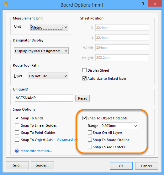
Hotspot Snap
Complimenting the real-time design rule engine, the Hotspot Snap feature overrides the snap grid, pulling the cursor to the hotspot of an electrical object that is within the hotspot snap range. This feature allows you to route from or to off-grid pads and vias.
The Hotspot Snap feature is enabled and the attraction range defined in the Board Options dialog (Home | Board | Board Options).
Real-time Design Rules
Underlying the PCB editor is a Design Rules engine that monitors editing actions in real time. Rather than needing to rely on a suitable snap grid setting to ensure objects are placed so they meet the design requirements, the rules engine immediately highlights a placement violation, or in the case of interactive routing, can prevent a placement violation. That means the snap grid can be set very small and objects can be placed as close as the design rules allow.